BCA 3RD SEM COA NOTES 2023-24
UNIT 1ST
Classification of Computers
The computer systems can be classified on the following basis:
1. On the basis of size.
2. On the basis of functionality.
3. On the basis of data handling.
Attention reader! All those who say programming isn't for kids, just haven't met the right mentors yet. Join the Demo Class for First Step to Coding Course, specifically designed for students of class 8 to 12.
The students will get to learn more about the world of programming in these free classes which will definitely help them in making a wise career choice in the future.
Classification on the basis of size
1. Super computers : The super computers are the most high performing system. A supercomputer is a computer with a high level of performance compared to a general-purpose computer. The actual Performance of a supercomputer is measured in FLOPS instead of MIPS. All of the world’s fastest 500 supercomputers run Linux-based operating systems. Additional research is being conducted in China, the US, the EU, Taiwan and Japan to build even faster, more high performing and more technologically superior supercomputers. Supercomputers actually play an important role in the field of computation, and are used for intensive computation tasks in various fields, including quantum mechanics, weather forecasting, climate research, oil and gas exploration, molecular modeling, and physical simulations. and also Throughout the history, supercomputers have been essential in the field of the cryptanalysis.
eg: PARAM, jaguar, roadrunner.
2. Mainframe computers : These are commonly called as big iron, they are usually used by big organisations for bulk data processing such as statics, census data processing, transaction processing and are widely used as the servers as these systems has a higher processing capability as compared to the other classes of computers, most of these mainframe architectures were established in 1960s, the research and development worked continuously over the years and the mainframes of today are far more better than the earlier ones, in size, capacity and efficiency.
Eg: IBM z Series, System z9 and System z10 servers.
3. Mini computers : These computers came into the market in mid 1960s and were sold at a much cheaper price than the main frames, they were actually designed for control, instrumentation, human interaction, and communication switching as distinct from calculation and record keeping, later they became very popular for personal uses with evolution.
In the 60s to describe the smaller computers that became possible with the use of transistors and core memory technologies, minimal instructions sets and less expensive peripherals such as the ubiquitous Teletype Model 33 ASR.They usually took up one or a few inch rack cabinets, compared with the large mainframes that could fill a room, there was a new term “MINICOMPUTERS” coined
Eg: Personal Laptop, PC etc.
4. Micro computers : A microcomputer is a small, relatively inexpensive computer with a microprocessor as its CPU. It includes a microprocessor, memory, and minimal I/O circuitry mounted on a single printed circuit board.The previous to these computers, mainframes and minicomputers, were comparatively much larger, hard to maintain and more expensive. They actually formed the foundation for present day microcomputers and smart gadgets that we use in day to day life.
Eg: Tablets, Smartwatches.
Classification on the basis of functionality
1. Servers : Servers are nothing but dedicated computers which are set-up to offer some services to the clients. They are named depending on the type of service they offered. Eg: security server, database server.
2. Workstation : Those are the computers designed to primarily to be used by single user at a time. They run multi-user operating systems. They are the ones which we use for our day to day personal / commercial work.
3. Information Appliances : They are the portable devices which are designed to perform a limited set of tasks like basic calculations, playing multimedia, browsing internet etc. They are generally referred as the mobile devices. They have very limited memory and flexibility and generally run on “as-is” basis.
4. Embedded computers : They are the computing devices which are used in other machines to serve limited set of requirements. They follow instructions from the non-volatile memory and they are not required to execute reboot or reset. The processing units used in such device work to those basic requirements only and are different from the ones that are used in personal computers- better known as workstations.
Classification on the basis of data handling
1. Analog : An analog computer is a form of computer that uses the continuously-changeable aspects of physical fact such as electrical, mechanical, or hydraulic quantities to model the problem being solved. Any thing that is variable with respect to time and continuous can be claimed as analog just like an analog clock measures time by means of the distance traveled for the spokes of the clock around the circular dial.
2. Digital : A computer that performs calculations and logical operations with quantities represented as digits, usually in the binary number system of “0” and “1”, “Computer capable of solving problems by processing information expressed in discrete form. from manipulation of the combinations of the binary digits, it can perform mathematical calculations, organize and analyze data, control industrial and other processes, and simulate dynamic systems such as global weather patterns.
3. Hybrid : A computer that processes both analog and digital data, Hybrid computer is a digital computer that accepts analog signals, converts them to digital and processes them in digital form.
Introduction of ALU
Representing and storing numbers were the basic operation of the computers of earlier times. The real go came when computation, manipulating numbers like adding, multiplying came into the picture. These operations are handled by the computer’s arithmetic logic unit (ALU). The ALU is the mathematical brain of a computer. The first ALU was INTEL 74181 implemented as a 7400 series is a TTL integrated circuit that was released in 1970.
The ALU is a digital circuit that provides arithmetic and logic operations. It is the fundamental building block of the central processing unit of a computer. A modern CPU has a very powerful ALU and it is complex in design. In addition to ALU modern CPU contains a control unit and a set of registers. Most of the operations are performed by one or more ALU’s, which load data from the input register. Registers are a small amount of storage available to the CPU. These registers can be accessed very fast. The control unit tells ALU what operation to perform on the available data. After calculation/manipulation, the ALU stores the output in an output register.
Introduction of Control Unit and its Design
Difficulty Level : Hard
Last Updated : 22 Aug, 2019
Control Unit is the part of the computer’s central processing unit (CPU), which directs the operation of the processor. It was included as part of the Von Neumann Architecture by John von Neumann. It is the responsibility of the Control Unit to tell the computer’s memory, arithmetic/logic unit and input and output devices how to respond to the instructions that have been sent to the processor. It fetches internal instructions of the programs from the main memory to the processor instruction register, and based on this register contents, the control unit generates a control signal that supervises the execution of these instructions.
A control unit works by receiving input information to which it converts into control signals, which are then sent to the central processor. The computer’s processor then tells the attached hardware what operations to perform. The functions that a control unit performs are dependent on the type of CPU because the architecture of CPU varies from manufacturer to manufacturer. Examples of devices that require a CU are:
Attention reader! Don’t stop learning now. Practice GATE exam well before the actual exam with the subject-wise and overall quizzes available in GATE Test Series Course.
Learn all GATE CS concepts with Free Live Classes on our youtube channel.
Control Processing Units(CPUs)
Graphics Processing Units(GPUs)
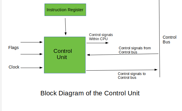
Functions of the Control Unit –
It coordinates the sequence of data movements into, out of, and between a processor’s many sub-units.
It interprets instructions.
It controls data flow inside the processor.
It receives external instructions or commands to which it converts to sequence of control signals.
It controls many execution units(i.e. ALU, data buffers and registers) contained within a CPU.
It also handles multiple tasks, such as fetching, decoding, execution handling and storing results.
Types of Control Unit –
There are two types of control units: Hardwired control unit and Microprogrammable control unit.
Hardwired Control Unit –
In the Hardwired control unit, the control signals that are important for instruction execution control are generated by specially designed hardware logical circuits, in which we can not modify the signal generation method without physical change of the circuit structure. The operation code of an instruction contains the basic data for control signal generation. In the instruction decoder, the operation code is decoded. The instruction decoder constitutes a set of many decoders that decode different fields of the instruction opcode.
As a result, few output lines going out from the instruction decoder obtains active signal values. These output lines are connected to the inputs of the matrix that generates control signals for executive units of the computer. This matrix implements logical combinations of the decoded signals from the instruction opcode with the outputs from the matrix that generates signals representing consecutive control unit states and with signals coming from the outside of the processor, e.g. interrupt signals. The matrices are built in a similar way as a programmable logic arrays.
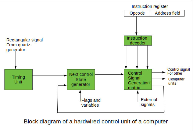
Control signals for an instruction execution have to be generated not in a single time point but during the entire time interval that corresponds to the instruction execution cycle. Following the structure of this cycle, the suitable sequence of internal states is organized in the control unit.
A number of signals generated by the control signal generator matrix are sent back to inputs of the next control state generator matrix. This matrix combines these signals with the timing signals, which are generated by the timing unit based on the rectangular patterns usually supplied by the quartz generator. When a new instruction arrives at the control unit, the control units is in the initial state of new instruction fetching. Instruction decoding allows the control unit enters the first state relating execution of the new instruction, which lasts as long as the timing signals and other input signals as flags and state information of the computer remain unaltered. A change of any of the earlier mentioned signals stimulates the change of the control unit state.
This causes that a new respective input is generated for the control signal generator matrix. When an external signal appears, (e.g. an interrupt) the control unit takes entry into a next control state that is the state concerned with the reaction to this external signal (e.g. interrupt processing). The values of flags and state variables of the computer are used to select suitable states for the instruction execution cycle.

The last states in the cycle are control states that commence fetching the next instruction of the program: sending the program counter content to the main memory address buffer register and next, reading the instruction word to the instruction register of computer. When the ongoing instruction is the stop instruction that ends program execution, the control unit enters an operating system state, in which it waits for a next user directive.
Microprogrammable control unit –
The fundamental difference between these unit structures and the structure of the hardwired control unit is the existence of the control store that is used for storing words containing encoded control signals mandatory for instruction execution.
In microprogrammed control units, subsequent instruction words are fetched into the instruction register in a normal way. However, the operation code of each instruction is not directly decoded to enable immediate control signal generation but it comprises the initial address of a microprogram contained in the control store.
With a single-level control store:
In this, the instruction opcode from the instruction register is sent to the control store address register. Based on this address, the first microinstruction of a microprogram that interprets execution of this instruction is read to the microinstruction register. This microinstruction contains in its operation part encoded control signals, normally as few bit fields. In a set microinstruction field decoders, the fields are decoded. The microinstruction also contains the address of the next microinstruction of the given instruction microprogram and a control field used to control activities of the microinstruction address generator.
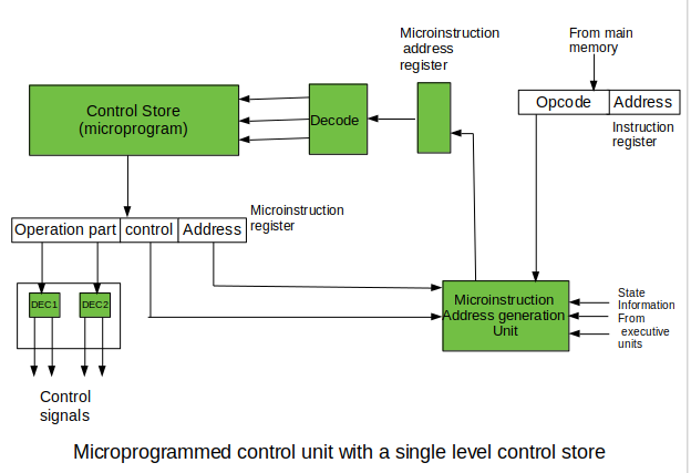
The last mentioned field decides the addressing mode (addressing operation) to be applied to the address embedded in the ongoing microinstruction. In microinstructions along with conditional addressing mode, this address is refined by using the processor condition flags that represent the status of computations in the current program. The last microinstruction in the instruction of the given microprogram is the microinstruction that fetches the next instruction from the main memory to the instruction register.
With a two-level control store:
In this, in a control unit with a two-level control store, besides the control memory for microinstructions, a nano-instruction memory is included. In such a control unit, microinstructions do not contain encoded control signals. The operation part of microinstructions contains the address of the word in the nano-instruction memory, which contains encoded control signals. The nano-instruction memory contains all combinations of control signals that appear in microprograms that interpret the complete instruction set of a given computer, written once in the form of nano-instructions.
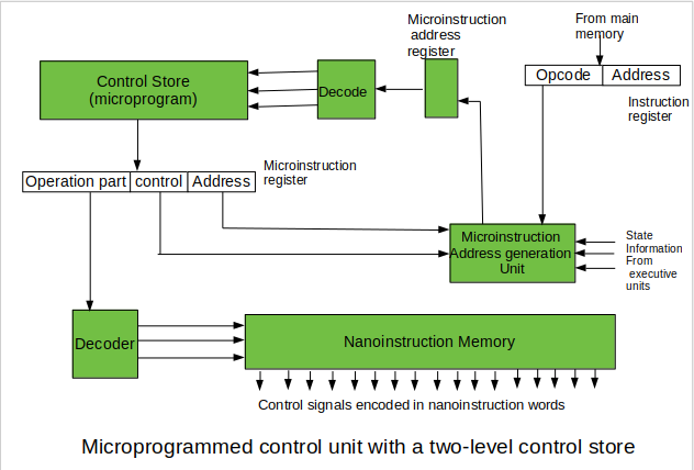
In this way, unnecessary storing of the same operation parts of microinstructions is avoided. In this case, microinstruction word can be much shorter than with the single level control store. It gives a much smaller size in bits of the microinstruction memory and, as a result, a much smaller size of the entire control memory. The microinstruction memory contains the control for selection of consecutive microinstructions, while those control signals are generated at the basis of nano-instructions. In nano-instructions, control signals are frequently encoded using 1 bit/ 1 signal method that eliminates decoding.
Von Neumann Architecture
Von Neumann architecture was first published by John von Neumann in 1945.
His computer architecture design consists of a Control Unit, Arithmetic and Logic Unit (ALU), Memory Unit, Registers and Inputs/Outputs.
Von Neumann architecture is based on the stored-program computer concept, where instruction data and program data are stored in the same memory. This design is still used in most computers produced today.

Central Processing Unit (CPU)
The Central Processing Unit (CPU) is the electronic circuit responsible for executing the instructions of a computer program.
It is sometimes referred to as the microprocessor or processor.
The CPU contains the ALU, CU and a variety of registers.
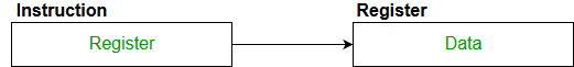
Registers
Registers are high speed storage areas in the CPU. All data must be stored in a register before it can be processed.
MAR Memory Address Register Holds the memory location of data that needs to be accessed
MDR Memory Data Register Holds data that is being transferred to or from memory
AC Accumulator Where intermediate arithmetic and logic results are stored
PC Program Counter Contains the address of the next instruction to be executed
CIR Current Instruction Register Contains the current instruction during processing
Arithmetic and Logic Unit (ALU)
The ALU allows arithmetic (add, subtract etc) and logic (AND, OR, NOT etc) operations to be carried out.
Control Unit (CU)
The control unit controls the operation of the computer’s ALU, memory and input/output devices, telling them how to respond to the program instructions it has just read and interpreted from the memory unit.
The control unit also provides the timing and control signals required by other computer components.
Buses
Buses are the means by which data is transmitted from one part of a computer to another, connecting all major internal components to the CPU and memory.
A standard CPU system bus is comprised of a control bus, data bus and address bus.
Address Bus Carries the addresses of data (but not the data) between the processor and memory
Data Bus Carries data between the processor, the memory unit and the input/output devices
Control Bus Carries control signals/commands from the CPU (and status signals from other devices) in order to control and coordinate all the activities within the computer
Memory Unit
The memory unit consists of RAM, sometimes referred to as primary or main memory. Unlike a hard drive (secondary memory), this memory is fast and also directly accessible by the CPU.
RAM is split into partitions. Each partition consists of an address and its contents (both in binary form).
The address will uniquely identify every location in the memory.
Loading data from permanent memory (hard drive), into the faster and directly accessible temporary memory (RAM), allows the CPU to operate much quicker.
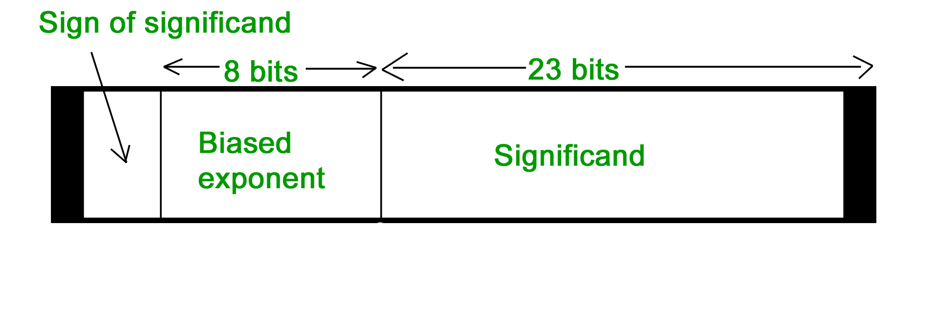
Introduction of Floating Point Representation
1. To convert the floating point into decimal, we have 3 elements in a 32-bit floating point representation:
i) Sign
ii) Exponent
iii) Mantissa
Attention reader! Don’t stop learning now. Get hold of all the important CS Theory concepts for SDE interviews with the CS Theory Course at a student-friendly price and become industry ready.
Sign bit is the first bit of the binary representation. ‘1’ implies negative number and ‘0’ implies positive number.
Example: 11000001110100000000000000000000 This is negative number.
Exponent is decided by the next 8 bits of binary representation. 127 is the unique number for 32 bit floating point representation. It is known as bias. It is determined by 2k-1 -1 where ‘k’ is the number of bits in exponent field.
There are 3 exponent bits in 8-bit representation and 8 exponent bits in 32-bit representation.
Thus
bias = 3 for 8 bit conversion (23-1 -1 = 4-1 = 3)
bias = 127 for 32 bit conversion. (28-1 -1 = 128-1 = 127)
Example: 01000001110100000000000000000000
10000011 = (131)10
131-127 = 4
Hence the exponent of 2 will be 4 i.e. 24 = 16.
Mantissa is calculated from the remaining 23 bits of the binary representation. It consists of ‘1’ and a fractional part which is determined by:
Example:
01000001110100000000000000000000
The fractional part of mantissa is given by:
1*(1/2) + 0*(1/4) + 1*(1/8) + 0*(1/16) +……… = 0.625
Thus the mantissa will be 1 + 0.625 = 1.625
The decimal number hence given as: Sign*Exponent*Mantissa = (-1)0*(16)*(1.625) = 26
2. To convert the decimal into floating point, we have 3 elements in a 32-bit floating point representation:
i) Sign (MSB)
ii) Exponent (8 bits after MSB)
iii) Mantissa (Remaining 23 bits)
Sign bit is the first bit of the binary representation. ‘1’ implies negative number and ‘0’ implies positive number.
Example: To convert -17 into 32-bit floating point representation Sign bit = 1
Exponent is decided by the nearest smaller or equal to 2n number. For 17, 16 is the nearest 2n. Hence the exponent of 2 will be 4 since 24 = 16. 127 is the unique number for 32 bit floating point representation. It is known as bias. It is determined by 2k-1 -1 where ‘k’ is the number of bits in exponent field.
Thus bias = 127 for 32 bit. (28-1 -1 = 128-1 = 127)
Now, 127 + 4 = 131 i.e. 10000011 in binary representation.
Mantissa: 17 in binary = 10001.
Move the binary point so that there is only one bit from the left. Adjust the exponent of 2 so that the value does not change. This is normalizing the number. 1.0001 x 24. Now, consider the fractional part and represented as 23 bits by adding zeros.
00010000000000000000000
Hardware Implementation
The hardware implementation of logic rnicrooperations requires that logic gates be inserted for each bit or pair of bits in the registers to perform the required logic function. Although there are 16 logic rnicrooperations, most computers use only four-AND, OR, XOR (exclusive-OR), and complementfrom which all others can be derived.
logic circuit: Figure 4-10 shows one stage of a circuit that generates the four basic logic rnicrooperations . It consists of four gates and a multiplexer. Each of the four logic operations is generated through a gate that performs the required logic. The outputs of the gates are applied to the data inputs of the multiplexer. The two selection inputs 51 and 50 choose one of the data inputs of the multiplexer and direct its value to the output. The diagram shows one typical stage with subscript i. For a logic circuit with n bits, the diagram must be repeated n times for i = 0, 1, 2, ... , n - 1. The selection variables are applied to all stages. The function table in Fig. 4-10(b) lists the logic rnicrooperations obtained for each combination of the selection variables.
Booth’s Algorithm
Booth algorithm gives a procedure for multiplying binary integers in signed 2’s complement representation in efficient way, i.e., less number of additions/subtractions required. It operates on the fact that strings of 0’s in the multiplier require no addition but just shifting and a string of 1’s in the multiplier from bit weight 2^k to weight 2^m can be treated as 2^(k+1 ) to 2^m.
As in all multiplication schemes, booth algorithm requires examination of the multiplier bits and shifting of the partial product. Prior to the shifting, the multiplicand may be added to the partial product, subtracted from the partial product, or left unchanged according to following rules:
Attention reader! Don’t stop learning now. Practice GATE exam well before the actual exam with the subject-wise and overall quizzes available in GATE Test Series Course.
Learn all GATE CS concepts with Free Live Classes on our youtube channel.
The multiplicand is subtracted from the partial product upon encountering the first least significant 1 in a string of 1’s in the multiplier
The multiplicand is added to the partial product upon encountering the first 0 (provided that there was a previous ‘1’) in a string of 0’s in the multiplier.
The partial product does not change when the multiplier bit is identical to the previous multiplier bit.
Hardware Implementation of Booths Algorithm – The hardware implementation of the booth algorithm requires the register configuration shown in the figure below.
Booth’s Algorithm Flowchart –
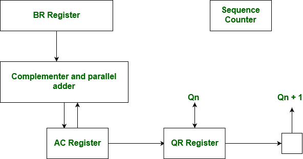
We name the register as A, B and Q, AC, BR and QR respectively. Qn designates the least significant bit of multiplier in the register QR. An extra flip-flop Qn+1is appended to QR to facilitate a double inspection of the multiplier.The flowchart for the booth algorithm is shown below.
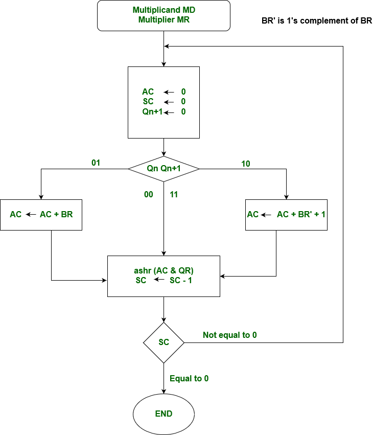
AC and the appended bit Qn+1 are initially cleared to 0 and the sequence SC is set to a number n equal to the number of bits in the multiplier. The two bits of the multiplier in Qn and Qn+1are inspected. If the two bits are equal to 10, it means that the first 1 in a string has been encountered. This requires subtraction of the multiplicand from the partial product in AC. If the 2 bits are equal to 01, it means that the first 0 in a string of 0’s has been encountered. This requires the addition of the multiplicand to the partial product in AC.
When the two bits are equal, the partial product does not change. An overflow cannot occur because the addition and subtraction of the multiplicand follow each other. As a consequence, the 2 numbers that are added always have a opposite signs, a condition that excludes an overflow. The next step is to shift right the partial product and the multiplier (including Qn+1). This is an arithmetic shift right (ashr) operation which AC and QR ti the right and leaves the sign bit in AC unchanged. The sequence counter is decremented and the computational loop is repeated n times.
Example – A numerical example of booth’s algorithm is shown below for n = 4. It shows the step by step multiplication of -5 and -7.MD = -5 = 1011, MD = 1011, MD'+1 = 0101 MR = -7 = 1001 The explanation of first step is as follows: Qn+1 AC = 0000, MR = 1001, Qn+1 = 0, SC = 4 Qn Qn+1 = 10 So, we do AC + (MD)'+1, which gives AC = 0101 On right shifting AC and MR, we get AC = 0010, MR = 1100 and Qn+1 = 1
Accumulator:
The accumulator is an 8-bit register (can store 8-bit data) that is the part of the arithmetic and logical unit (ALU). After performing arithmetical or logical operations, the result is stored in accumulator. Accumulator is also defined as register A.
Computer Organization | RISC and CISC
Reduced Instruction Set Architecture (RISC) –
The main idea behind is to make hardware simpler by using an instruction set composed of a few basic steps for loading, evaluating, and storing operations just like a load command will load data, store command will store the data.
Complex Instruction Set Architecture (CISC) –
The main idea is that a single instruction will do all loading, evaluating, and storing operations just like a multiplication command will do stuff like loading data, evaluating, and storing it, hence it’s complex.
Both approaches try to increase the CPU performance
RISC: Reduce the cycles per instruction at the cost of the number of instructions per program.
CISC: The CISC approach attempts to minimize the number of instructions per program but at the cost of increase in number of cycles per instruction.
Earlier when programming was done using assembly language, a need was felt to make instruction do more tasks because programming in assembly was tedious and error-prone due to which CISC architecture evolved but with the uprise of high-level language dependency on assembly reduced RISC architecture prevailed.
Characteristic of RISC –
Simpler instruction, hence simple instruction decoding.
Instruction comes undersize of one word.
Instruction takes a single clock cycle to get executed.
More general-purpose registers.
Simple Addressing Modes.
Less Data types.
Pipeline can be achieved.
Characteristic of CISC –
Complex instruction, hence complex instruction decoding.
Instructions are larger than one-word size.
Instruction may take more than a single clock cycle to get executed.
Less number of general-purpose registers as operation get performed in memory itself.
Complex Addressing Modes.
More Data types.
Example – Suppose we have to add two 8-bit number:
CISC approach: There will be a single command or instruction for this like ADD which will perform the task.
RISC approach: Here programmer will write the first load command to load data in registers then it will use a suitable operator and then it will store the result in the desired location.
So, add operation is divided into parts i.e. load, operate, store due to which RISC programs are longer and require more memory to get stored but require fewer transistors due to less complex command.
Difference –
RISCCISCFocus on software Focus on hardware
Uses only Hardwired control unit Uses both hardwired and micro programmed control unit
Transistors are used for more registers Transistors are used for storing complex
Instructions
Fixed sized instructions Variable sized instructions
Can perform only Register to Register Arithmetic operations Can perform REG to REG or REG to MEM or MEM to MEM
Requires more number of registers Requires less number of registers
Code size is large Code size is small
An instruction execute in a single clock cycle Instruction takes more than one clock cycle
An instruction fit in
one word Instructions are larger than the size of one word
Computer Organization | Instruction Formats (Zero, One, Two and Three Address Instruction)
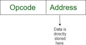
A computer performs a task based on the instruction provided. Instruction in computers comprises groups called fields. These fields contain different information as for computers everything is in 0 and 1 so each field has different significance based on which a CPU decides what to perform. The most common fields are:
Operation field specifies the operation to be performed like addition.
Address field which contains the location of the operand, i.e., register or memory location.
Mode field which specifies how operand is to be founded.
Instruction is of variable length depending upon the number of addresses it contains. Generally, CPU organization is of three types based on the number of address fields:
Single Accumulator organization
General register organization
Stack organization
In the first organization, the operation is done involving a special register called the accumulator. In second on multiple registers are used for the computation purpose. In the third organization the work on stack basis operation due to which it does not contain any address field. Only a single organization doesn’t need to be applied, a blend of various organizations is mostly what we see generally.
Based on the number of address, instructions are classified as:
Note that we will use X = (A+B)*(C+D) expression to showcase the procedure.
Zero Address Instructions –
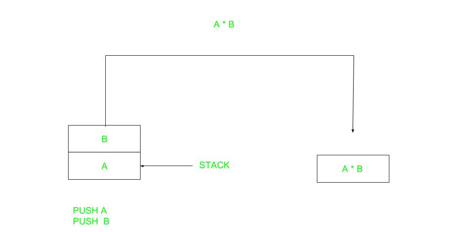
A stack-based computer does not use the address field in the instruction. To evaluate an expression first it is converted to reverse Polish Notation i.e. Postfix Notation. Expression: X = (A+B)*(C+D) Postfixed : X = AB+CD+* TOP means top of stack M[X] is any memory location
PUSH A TOP = A
PUSH B TOP = B
ADD TOP = A+B
PUSH C TOP = C
PUSH D TOP = D
ADD TOP = C+D
MUL TOP = (C+D)*(A+B)
POP X M[X] = TOP
2 .One Address Instructions –
This uses an implied ACCUMULATOR register for data manipulation. One operand is in the accumulator and the other is in the register or memory location. Implied means that the CPU already knows that one operand is in the accumulator so there is no need to specify it.
 Expression: X = (A+B)*(C+D)
AC is accumulator
M[] is any memory location
M[T] is temporary location
Expression: X = (A+B)*(C+D)
AC is accumulator
M[] is any memory location
M[T] is temporary locationLOAD A AC = M[A]
ADD B AC = AC + M[B]
STORE T M[T] = AC
LOAD C AC = M[C]
ADD D AC = AC + M[D]
MUL T AC = AC * M[T]
STORE X M[X] = AC
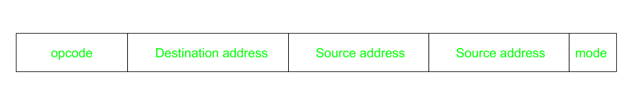
3.Two Address Instructions –
This is common in commercial computers. Here two addresses can be specified in the instruction. Unlike earlier in one address instruction, the result was stored in the accumulator, here the result can be stored at different locations rather than just accumulators, but require more number of bit to represent address.

Here destination address can also contain operand. Expression: X = (A+B)*(C+D) R1, R2 are registers M[] is any memory location
MOV R1, A R1 = M[A]
ADD R1, B R1 = R1 + M[B]
MOV R2, C R2 = C
ADD R2, D R2 = R2 + D
MUL R1, R2 R1 = R1 * R2
MOV X, R1 M[X] = R1
4.Three Address Instructions –
This has three address field to specify a register or a memory location. Program created are much short in size but number of bits per instruction increase. These instructions make creation of program much easier but it does not mean that program will run much faster because now instruction only contain more information but each micro operation (changing content of register, loading address in address bus etc.) will be performed in one cycle only.
 Expression: X = (A+B)*(C+D)
R1, R2 are registers
M[] is any memory location
Expression: X = (A+B)*(C+D)
R1, R2 are registers
M[] is any memory locationADD R1, A, B R1 = M[A] + M[B]
ADD R2, C, D R2 = M[C] + M[D]
MUL X, R1, R2 M[X] = R1 * R2
UNIT 2
Introduction to Parallel Computing
Before taking a toll on Parallel Computing, first, let’s take a look at the background of computations of computer software and why it failed for the modern era.
Computer software was written conventionally for serial computing. This meant that to solve a problem, an algorithm divides the problem into smaller instructions. These discrete instructions are then executed on the Central Processing Unit of a computer one by one. Only after one instruction is finished, next one starts.
A real-life example of this would be people standing in a queue waiting for a movie ticket and there is only a cashier. The cashier is giving tickets one by one to the persons. The complexity of this situation increases when there are 2 queues and only one cashier.
So, in short, Serial Computing is following:
In this, a problem statement is broken into discrete instructions.
Then the instructions are executed one by one.
Only one instruction is executed at any moment of time.
Look at point 3. This was causing a huge problem in the computing industry as only one instruction was getting executed at any moment of time. This was a huge waste of hardware resources as only one part of the hardware will be running for particular instruction and of time. As problem statements were getting heavier and bulkier, so does the amount of time in execution of those statements. Examples of processors are Pentium 3 and Pentium 4.
Now let’s come back to our real-life problem. We could definitely say that complexity will decrease when there are 2 queues and 2 cashiers giving tickets to 2 persons simultaneously. This is an example of Parallel Computing.
Parallel Computing :
It is the use of multiple processing elements simultaneously for solving any problem. Problems are broken down into instructions and are solved concurrently as each resource that has been applied to work is working at the same time.
Advantages of Parallel Computing over Serial Computing are as follows:
It saves time and money as many resources working together will reduce the time and cut potential costs.
It can be impractical to solve larger problems on Serial Computing.
It can take advantage of non-local resources when the local resources are finite.
Serial Computing ‘wastes’ the potential computing power, thus Parallel Computing makes better work of the hardware.
Types of Parallelism:
Bit-level parallelism –
It is the form of parallel computing which is based on the increasing processor’s size. It reduces the number of instructions that the system must execute in order to perform a task on large-sized data.
Example: Consider a scenario where an 8-bit processor must compute the sum of two 16-bit integers. It must first sum up the 8 lower-order bits, then add the 8 higher-order bits, thus requiring two instructions to perform the operation. A 16-bit processor can perform the operation with just one instruction.
Instruction-level parallelism –
A processor can only address less than one instruction for each clock cycle phase. These instructions can be re-ordered and grouped which are later on executed concurrently without affecting the result of the program. This is called instruction-level parallelism.
Task Parallelism –
Task parallelism employs the decomposition of a task into subtasks and then allocating each of the subtasks for execution. The processors perform the execution of sub-tasks concurrently.
4. Data-level parallelism (DLP) –
Instructions from a single stream operate concurrently on several data – Limited by non-regular data manipulation patterns and by memory bandwidth
Why parallel computing?
The whole real-world runs in dynamic nature i.e. many things happen at a certain time but at different places concurrently. This data is extensively huge to manage.
Real-world data needs more dynamic simulation and modeling, and for achieving the same, parallel computing is the key.
Parallel computing provides concurrency and saves time and money.
Complex, large datasets, and their management can be organized only and only using parallel computing’s approach.
Ensures the effective utilization of the resources. The hardware is guaranteed to be used effectively whereas in serial computation only some part of the hardware was used and the rest rendered idle.
Also, it is impractical to implement real-time systems using serial computing.
Applications of Parallel Computing:
Databases and Data mining.
Real-time simulation of systems.
Science and Engineering.
Advanced graphics, augmented reality, and virtual reality.
Limitations of Parallel Computing:
It addresses such as communication and synchronization between multiple sub-tasks and processes which is difficult to achieve.
The algorithms must be managed in such a way that they can be handled in a parallel mechanism.
The algorithms or programs must have low coupling and high cohesion. But it’s difficult to create such programs.
More technically skilled and expert programmers can code a parallelism-based program well.
Future of Parallel Computing: The computational graph has undergone a great transition from serial computing to parallel computing. Tech giant such as Intel has already taken a step towards parallel computing by employing multicore processors. Parallel computation will revolutionize the way computers work in the future, for the better good. With all the world connecting to each other even more than before, Parallel Computing does a better role in helping us stay that way. With faster networks, distributed systems, and multi-processor computers, it becomes even more necessary.
Architecture of 8086
A Microprocessor is an Integrated Circuit with all the functions of a CPU however, it cannot be used stand alone since unlike a microcontroller it has no memory or peripherals.
8086 does not have a RAM or ROM inside it. However, it has internal registers for storing intermediate and final results and interfaces with memory located outside it through the System Bus.
In case of 8086, it is a 16-bit Integer processor in a 40 pin, Dual Inline Packaged IC.
The size of the internal registers(present within the chip) indicate how much information the processor can operate on at a time (in this case 16-bit registers) and how it moves data around internally within the chip, sometimes also referred to as the internal data bus.
8086 provides the programmer with 14 internal registers, each 16 bits or 2 Bytes wide.
Memory segmentation:
To increase execution speed and fetching speed, 8086 segments the memory.
It’s 20 bit address bus can address 1MB of memory, it segments it into 16 64kB segments.
8086 works only with four 64KB segments within the whole 1MB memory.
The internal architecture of Intel 8086 is divided into 2 units: The Bus Interface Unit (BIU), and The Execution Unit (EU). These are explained as following below.
1. The Bus Interface Unit (BIU):
It provides the interface of 8086 to external memory and I/O devices via the System Bus. It performs various machine cycles such as memory read, I/O read etc. to transfer data between memory and I/O devices.
BIU performs the following functions-
It generates the 20 bit physical address for memory access.
It fetches instructions from the memory.
It transfers data to and from the memory and I/O.
Maintains the 6 byte prefetch instruction queue(supports pipelining).
BIU mainly contains the 4 Segment registers, the Instruction Pointer, a prefetch queue and an Address Generation Circuit.
Instruction Pointer (IP):
It is a 16 bit register. It holds offset of the next instructions in the Code Segment.
IP is incremented after every instruction byte is fetched.
IP gets a new value whenever a branch instruction occurs.
CS is multiplied by 10H to give the 20 bit physical address of the Code Segment.
Address of the next instruction is calculated as CS x 10H + IP.
Example: CS = 4321H IP = 1000H then CS x 10H = 43210H + offset = 44210H
This is the address of the instruction.
Code Segment register:
CS holds the base address for the Code Segment. All programs are stored in the Code Segment and accessed via the IP.
Data Segment register:
DS holds the base address for the Data Segment.
Stack Segment register:
SS holds the base address for the Stack Segment.
Extra Segment register:
ES holds the base address for the Extra Segment.
Address Generation Circuit:
The BIU has a Physical Address Generation Circuit.
It generates the 20 bit physical address using Segment and Offset addresses using the formula:
Physical Address = Segment Address x 10H + Offset Address
6 Byte Pre-fetch Queue:
It is a 6 byte queue (FIFO).
Fetching the next instruction (by BIU from CS) while executing the current instruction is called pipelining.
Gets flushed whenever a branch instruction occurs.
2. The Execution Unit (EU):
The main components of the EU are General purpose registers, the ALU, Special purpose registers, Instruction Register and Instruction Decoder and the Flag/Status Register.
Fetches instructions from the Queue in BIU, decodes and executes arithmetic and logic operations using the ALU.
Sends control signals for internal data transfer operations within the microprocessor.
Sends request signals to the BIU to access the external module.
It operates with respect to T-states (clock cycles) and not machine cycles.
8086 has four 16 bit general purpose registers AX, BX, CX and DX. Store intermediate values during execution. Each of these have two 8 bit parts (higher and lower).
AX – This is the accumulator. It is of 16 bits and is divided into two 8-bit registers AH and AL to also perform 8-bit instructions.
It is generally used for arithmetical and logical instructions but in 8086 microprocessor it is not mandatory to have accumulator as the destination operand.
Example:ADD AX, AX (AX = AX + AX)
BX – This is the base register. It is of 16 bits and is divided into two 8-bit registers BH and BL to also perform 8-bit instructions.
It is used to store the value of the offset.
Example:MOV BL, [500] (BL = 500H)
CX – This is the counter register. It is of 16 bits and is divided into two 8-bit registers CH and CL to also perform 8-bit instructions.
It is used in looping and rotation.
Example:MOV CX, 0005 LOOP
DX – This is the data register. It is of 16 bits and is divided into two 8-bit registers DH and DL to also perform 8-bit instructions.
It is used in multiplication an input/output port addressing.
Example:MUL BX (DX, AX = AX * BX)
SP – This is the stack pointer. It is of 16 bits.
It points to the topmost item of the stack. If the stack is empty the stack pointer will be (FFFE)H. It’s offset address relative to stack segment.
BP – This is the base pointer. It is of 16 bits.
It is primary used in accessing parameters passed by the stack. It’s offset address relative to stack segment.
SI – This is the source index register. It is of 16 bits.
It is used in the pointer addressing of data and as a source in some string related operations. It’s offset is relative to data segment.
DI – This is the destination index register. It is of 16 bits.
It is used in the pointer addressing of data and as a destination in some string related operations.It’s offset is relative to extra segment.
Arithmetic Logic Unit (16 bit):
Performs 8 and 16 bit arithmetic and logic operations.
Special purpose registers (16-bit):
Stack Pointer:
Points to Stack top. Stack is in Stack Segment, used during instructions like PUSH, POP, CALL, RET etc.
Base Pointer:
BP can hold offset address of any location in the stack segment. It is used to access random locations of the stack.
Source Index:
It holds offset address in Data Segment during string operations.
Destination Index:
It holds offset address in Extra Segment during string operations.
Instruction Register and Instruction Decoder:
The EU fetches an opcode from the queue into the instruction register. The instruction decoder decodes it and sends the information to the control circuit for execution.
Flag/Status register (16 bits):
It has 9 flags that help change or recognize the state of the microprocessor.
6 Status flags:
carry flag(CF)
parity flag(PF)
auxiliary carry flag(AF)
zero flag(Z)
sign flag(S)
overflow flag (O)
Status flags are updated after every arithmetic and logic operation.
3 Control flags:
trap flag(TF)
interrupt flag(IF)
direction flag(DF)
These flags can be set or reset using control instructions like CLC, STC, CLD, STD, CLI, STI, etc.
The Control flags are used to control certain operations.
UNIT 2
Processor Organization
Introduction to Parallelism
Computer software was written conventionally for serial computing. This meant that to solve a problem, an algorithm divides the problem into smaller instructions. These discrete instructions are then executed on the Central Processing Unit of a computer one by one. Only after one instruction is finished, next one starts.
A real-life example of this would be people standing in a queue waiting for a movie ticket and there is only a cashier. The cashier is giving tickets one by one to the persons. The complexity of this situation increases when there are 2 queues and only one cashier.
Parallel Computing :
It is the use of multiple processing elements simultaneously for solving any problem. Problems are broken down into instructions and are solved concurrently as each resource that has been applied to work is working at the same time.
Advantages of Parallel Computing over Serial Computing are as follows:
It saves time and money as many resources working together will reduce the time and cut potential costs.
It can be impractical to solve larger problems on Serial Computing.
It can take advantage of non-local resources when the local resources are finite.
Serial Computing ‘wastes’ the potential computing power, thus Parallel Computing makes better work of the hardware.
Types of Parallelism:
Bit-level parallelism –
It is the form of parallel computing which is based on the increasing processor’s size. It reduces the number of instructions that the system must execute in order to perform a task on large-sized data.
Example: Consider a scenario where an 8-bit processor must compute the sum of two 16-bit integers. It must first sum up the 8 lower-order bits, then add the 8 higher-order bits, thus requiring two instructions to perform the operation. A 16-bit processor can perform the operation with just one instruction.
Instruction-level parallelism –
A processor can only address less than one instruction for each clock cycle phase. These instructions can be re-ordered and grouped which are later on executed concurrently without affecting the result of the program. This is called instruction-level parallelism.
Task Parallelism –
Task parallelism employs the decomposition of a task into subtasks and then allocating each of the subtasks for execution. The processors perform the execution of sub-tasks concurrently.
4. Data-level parallelism (DLP) –
Instructions from a single stream operate concurrently on several data – Limited by non-regular data manipulation patterns and by memory bandwidth
Computer Arithmetic
Sign Magnitude
Sign magnitude is a very simple representation of negative numbers. In sign magnitude the first bit is dedicated to represent the sign and hence it is called sign bit.
Sign bit ‘1’ represents negative sign.
Sign bit ‘0’ represents positive sign.
In sign magnitude representation of a n – bit number, the first bit will represent sign and rest n-1 bits represent magnitude of number.
For example,
+25 = 011001
Where 11001 = 25
And 0 for ‘+’
-25 = 111001
Where 11001 = 25
And 1 for ‘-‘.
Range of number represented by sign magnitude method = -(2n-1-1) to +(2n-1-1) (for n bit number)
But there is one problem in sign magnitude and that is we have two representations of 0
+0 = 000000
– 0 = 100000
2’s complement method
To represent a negative number in this form, first we need to take the 1’s complement of the number represented in simple positive binary form and then add 1 to it.
For example:
(-8)10 = (1000)2
1’s complement of 1000 = 0111
Adding 1 to it, 0111 + 1 = 1000
So, (-8)10 = (1000)2
Please don’t get confused with (8)10 =1000 and (-8)10=1000 as with 4 bits, we can’t represent a positive number more than 7. So, 1000 is representing -8 only.
Range of number represented by 2’s complement = (-2n-1 to 2n-1 – 1)
Floating point representation of numbers
32-bit representation floating point numbers IEEE standard
Normalization
Floating point numbers are usually normalized
Exponent is adjusted so that leading bit (MSB) of mantissa is 1
Since it is always 1 there is no need to store it
Scientific notation where numbers are normalized to give a single digit before the decimal point like in decimal system e.g. 3.123 x 10³
For example, we represent 3.625 in 32 bit format.
Changing 3 in binary=11
Changing .625 in binary
.625 X 2 1
.25 X 2 0
.5 X 2 1
Writing in binary exponent form
3.625=11.101 X 20
On normalizing
11.101 X 20=1.1101 X 21
On biasing exponent = 127 + 1 = 128
(128)10=(10000000) 2
For getting significand
Digits after decimal = 1101
Expanding to 23 bit = 11010000000000000000000
Setting sign bit
As it is a positive number, sign bit = 0
Finally we arrange according to representation
Sign bit exponent significand 0 10000000 11010000000000000000000
64-bit representation floating point numbers IEEE standard
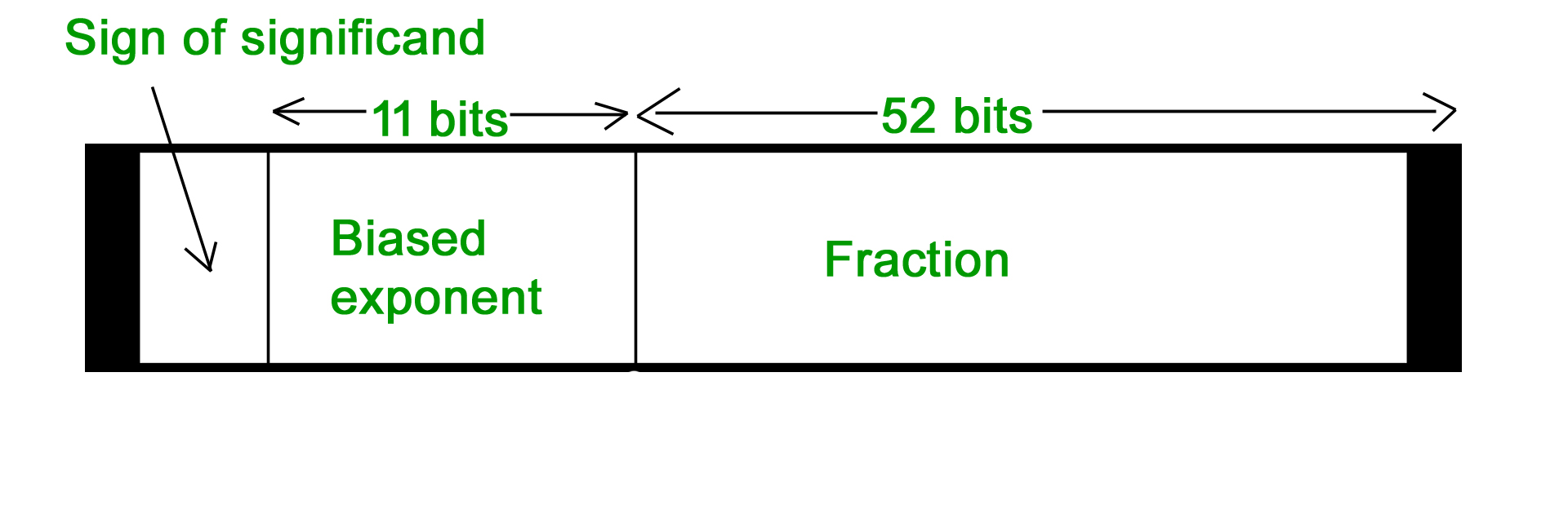
Again we follow the same procedure upto normalization. After that, we add 1023 to bias the exponent.
For example, we represent -3.625 in 64 bit format.
Changing 3 in binary = 11
Changing .625 in binary.625 X 2 1 .25 X 2 0 .5 X 2 1
Writing in binary exponent form
3.625 = 11.101 X 20
On normalizing
11.101 X 20 = 1.1101 X 21
On biasing exponent 1023 + 1 = 1024
(1024)10 = (10000000000)2
So 11 bit exponent = 10000000000
52 bit significand = 110100000000 …………. making total 52 bits
Setting sign bit = 1 (number is negative)
So, final representation
1 10000000000 110100000000 …………. making total 52 bits by adding further 0’s
Converting floating point into decimal
Let’s convert a FP number into decimal
1 01111100 11000000000000000000000
Floating Point Representation
To convert the floating point into decimal, we have 3 elements in a 32-bit floating point representation:
i) Sign
ii) Exponent
iii) Mantissa
Sign bit is the first bit of the binary representation. ‘1’ implies negative number and ‘0’ implies positive number.
Example: 11000001110100000000000000000000 This is negative number.
Exponent is decided by the next 8 bits of binary representation. 127 is the unique number for 32 bit floating point representation. It is known as bias. It is determined by 2k-1 -1 where ‘k’ is the number of bits in exponent field.
There are 3 exponent bits in 8-bit representation and 8 exponent bits in 32-bit representation.
Thus
bias = 3 for 8 bit conversion (23-1 -1 = 4-1 = 3)
bias = 127 for 32 bit conversion. (28-1 -1 = 128-1 = 127)
Example: 01000001110100000000000000000000
10000011 = (131)10
131-127 = 4
Hence the exponent of 2 will be 4 i.e. 24 = 16.
Mantissa is calculated from the remaining 23 bits of the binary representation. It consists of ‘1’ and a fractional part which is determined by:
Example:
01000001110100000000000000000000
The fractional part of mantissa is given by:
1*(1/2) + 0*(1/4) + 1*(1/8) + 0*(1/16) +……… = 0.625
Thus the mantissa will be 1 + 0.625 = 1.625
Architecture of 8086
A Microprocessor is an Integrated Circuit with all the functions of a CPU however, it cannot be used stand alone since unlike a microcontroller it has no memory or peripherals.
8086 does not have a RAM or ROM inside it. However, it has internal registers for storing intermediate and final results and interfaces with memory located outside it through the System Bus.
In case of 8086, it is a 16-bit Integer processor in a 40 pin, Dual Inline Packaged IC.
The size of the internal registers(present within the chip) indicate how much information the processor can operate on at a time (in this case 16-bit registers) and how it moves data around internally within the chip, sometimes also referred to as the internal data bus.
8086 provides the programmer with 14 internal registers, each 16 bits or 2 Bytes wide.
The Bus Interface Unit (BIU):
It provides the interface of 8086 to external memory and I/O devices via the System Bus. It performs various machine cycles such as memory read, I/O read etc. to transfer data between memory and I/O devices.
BIU performs the following functions-
It generates the 20 bit physical address for memory access.
It fetches instructions from the memory.
It transfers data to and from the memory and I/O.
Maintains the 6 byte prefetch instruction queue(supports pipelining).
BIU mainly contains the 4 Segment registers, the Instruction Pointer, a prefetch queue and an Address Generation Circuit.
Instruction Pointer (IP):
It is a 16 bit register. It holds offset of the next instructions in the Code Segment.
IP is incremented after every instruction byte is fetched.
IP gets a new value whenever a branch instruction occurs.
CS is multiplied by 10H to give the 20 bit physical address of the Code Segment.
Address of the next instruction is calculated as CS x 10H + IP.
Example: CS = 4321H IP = 1000H then CS x 10H = 43210H + offset = 44210H
This is the address of the instruction.
Code Segment register:
CS holds the base address for the Code Segment. All programs are stored in the Code Segment and accessed via the IP.
Data Segment register:
DS holds the base address for the Data Segment.
Stack Segment register:
SS holds the base address for the Stack Segment.
Extra Segment register:
ES holds the base address for the Extra Segment.
Address Generation Circuit:
The BIU has a Physical Address Generation Circuit.
It generates the 20 bit physical address using Segment and Offset addresses using the formula:
Physical Address = Segment Address x 10H + Offset Address
6 Byte Pre-fetch Queue:
It is a 6 byte queue (FIFO).
Fetching the next instruction (by BIU from CS) while executing the current instruction is called pipelining.
Gets flushed whenever a branch instruction occurs.
2. The Execution Unit (EU):
The main components of the EU are General purpose registers, the ALU, Special purpose registers, Instruction Register and Instruction Decoder and the Flag/Status Register.
Fetches instructions from the Queue in BIU, decodes and executes arithmetic and logic operations using the ALU.
Sends control signals for internal data transfer operations within the microprocessor.
Sends request signals to the BIU to access the external module.
It operates with respect to T-states (clock cycles) and not machine cycles.
8086 has four 16 bit general purpose registers AX, BX, CX and DX. Store intermediate values during execution. Each of these have two 8 bit parts (higher and lower)
AX register:
It holds operands and results during multiplication and division operations. Also an accumulator during String operations.
BX register:
It holds the memory address (offset address) in indirect addressing modes.
CX register:
It holds count for instructions like loop, rotate, shift and string operations.
DX register:
It is used with AX to hold 32 bit values during multiplication and division.
Arithmetic Logic Unit (16 bit):
Performs 8 and 16 bit arithmetic and logic operations.
Special purpose registers (16-bit):
Stack Pointer:
Points to Stack top. Stack is in Stack Segment, used during instructions like PUSH, POP, CALL, RET etc.
Base Pointer:
BP can hold offset address of any location in the stack segment. It is used to access random locations of the stack.
Source Index:
It holds offset address in Data Segment during string operations.
Destination Index:
It holds offset address in Extra Segment during string operations.
Instruction Register and Instruction Decoder:
The EU fetches an opcode from the queue into the instruction register. The instruction decoder decodes it and sends the information to the control circuit for execution.
Flag/Status register (16 bits):
It has 9 flags that help change or recognize the state of the microprocessor.
6 Status flags:
carry flag(CF)
parity flag(PF)
auxiliary carry flag(AF)
zero flag(Z)
sign flag(S)
overflow flag (O)
Status flags are updated after every arithmetic and logic operation.
3 Control flags:
trap flag(TF)
interrupt flag(IF)
direction flag(DF)
These flags can be set or reset using control instructions like CLC, STC, CLD, STD, CLI, STI, etc.
The Control flags are used to control certain operations.
Register Organization
Register organization is the arrangement of the registers in the processor. The processor designers decide the organization of the registers in a processor. Different processors may have different register organization. Depending on the roles played by the registers they can be categorized into two types, user-visible register and control and status register
What is Register?
Registers are the smaller and the fastest accessible memory units in the central processing unit (CPU). According to memory hierarchy, the registers in the processor, function a level above the main memory and cache memory. The registers used by the central unit are also called as processor registers.
A register can hold the instruction, address location, or operands. Sometimes, the instruction has register as a part of itself.
Types of Registers
As we have discussed above, registers can be organized into two main categories i.e. the User-Visible Registers and the Control and Status Registers. Although we can’t separate the registers in the processors clearly among these two categories.
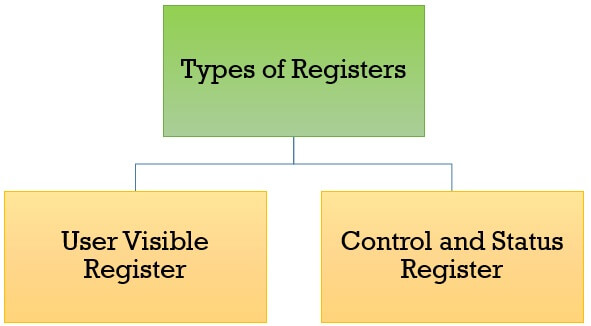
This is because in some processors, a register may be user-visible and in some, the same may not be user-visible. But for our rest of discussion regarding register organization, we will consider these two categories of register.
User Visible Registers
General Purpose Register
Data Register
Address Register
Condition Codes
Control and Status Registers
Program Counter
Instruction Register
Memory Address Register
Memory Buffer Register
User-Visible Registers
These registers are visible to the assembly or machine language programmers and they use them effectively to minimize the memory references in the instructions. Well, these registers can only be referenced using the machine or assembly language.
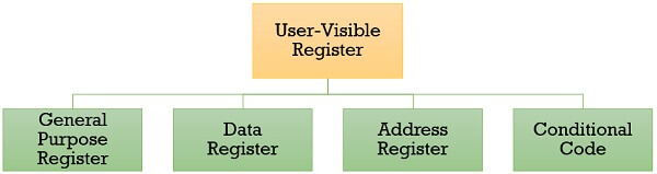
The registers that fall in this category are discussed below:
1. General Purpose Register
The general-purpose registers detain both the addresses or the data. Although we have separate data registers and address registers. The general purpose register also accepts the intermediate results in the course of program execution.
Well, the programmers can restrict some of the general-purpose registers to specific functions. Like, some registers are specifically used for stack operations or for floating-point operations. The general-purpose register can also be employed for the addressing functions.
2. Data Register
The term itself describes that these registers are employed to hold the data. But the programmers can’t use these registers for calculating operand address.
3. Address Register
Now, the address registers contain the address of an operand or it can also act as a general-purpose register. An address register may be dedicated to a certain addressing mode. Let us understand this with the examples.
(a) Segment Pointer Register
A memory divided in segments, requires a segment register to hold the base address of the segment. There can be multiple segment registers. As one segment register can be employed to hold the base address of the segment occupied by the operating system. The other segment register can hold the base address of the segment allotted to the processor.
(b) Index Register
The index register is employed for indexed addressing and it is initial value is 0. Generally, it used for traversing the memory locations. After each reference, the index register is incremented or decremented by 1, depending upon the nature of the operation.
Sometime the index register may be auto indexed.
(c) Stack Pointer Register
The stack register has the address that points the stack top.
4. Condition Code
Condition codes are the flag bits which are the part of the control register. The condition codes are set by the processor as a result of an operation and they are implicitly read through the machine instruction.
The programmers are not allowed to alter the conditional codes. Generally, the condition codes are tested during conditional branch operation.
Control and Status Registers
The control and status register holds the address or data that is important to control the processor’s operation. The most important thing is that these registers are not visible to the users. Below we will discuss all the control and status registers are essential for the execution of an instruction.
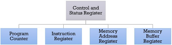
1. Program Counter
The program counter is a processor register that holds the address of the instruction that has to be executed next. It is a processor which updates the program counter with the address of the next instruction to be fetched for execution.
2. Instruction Register
Instruction register has the instruction that is currently fetched. It helps in analyzing the opcode and operand present in the instruction.
3. Memory Address Register (MAR)
Memory address register holds the address of a memory location.
4. Memory Buffer Register (MBR)
The memory buffer register holds the data that has to be written to a memory location or it holds the data that is recently been read.
The memory address registers (MAR) and memory buffer registers (MBR) are used to move the data between processor and memory.
A part from the above registers, several processors have a register termed as Program Status Word (PSW). As the word suggests it contains the status information.
The fields included in Program Status Word (PSW):
Sign: This field has the resultant sign bit of the last arithmetic operation performed.
Zero: This field is set when the result of the operation is zero.
Carry: This field is set when an arithmetic operation results in a carry into or borrow out.
Equal: If a logical operation results in, equality the Equal bit is set.
Overflow: This bit indicates the arithmetic overflow.
Interrupt: This bit is set to enable or disable the interrupts.
Supervisor: This bit indicates whether the processor is executing in the supervisor mode or the user mode.
So, these are the types of registers a processor has. The processor designer organizes the registers according to the requirement of the processor.
Addressing Modes
Addressing Modes– The term addressing modes refers to the way in which the operand of an instruction is specified. The addressing mode specifies a rule for interpreting or modifying the address field of the instruction before the operand is actually executed.
Addressing modes for 8086 instructions are divided into two categories:
Addressing modes for data
2) Addressing modes for branch
The 8086 memory addressing modes provide flexible access to memory, allowing you to easily access variables, arrays, records, pointers, and other complex data types. The key to good assembly language programming is the proper use of memory addressing modes.
An assembly language program instruction consists of two parts

The memory address of an operand consists of two components:
IMPORTANT TERMS
Starting address of memory segment.
Effective address or Offset: An offset is determined by adding any combination of three address elements: displacement, base and index.
Displacement: It is an 8 bit or 16 bit immediate value given in the instruction.
Base: Contents of base register, BX or BP.
Index: Content of index register SI or DI.
According to different ways of specifying an operand by 8086 microprocessor, different addressing modes are used by 8086.
Addressing modes used by 8086 microprocessor are discussed below:
Implied mode:: In implied addressing the operand is specified in the instruction itself. In this mode the data is 8 bits or 16 bits long and data is the part of instruction. Zero address instruction are designed with implied addressing mode.
Example: CLC (used to reset Carry flag to 0)
Immediate addressing mode (symbol #):In this mode data is present in address field of instruction .Designed like one address instruction format.
Note:Limitation in the immediate mode is that the range of constants are restricted by size of address field.
 Example: MOV AL, 35H (move the data 35H into AL register)
Register mode: In register addressing the operand is placed in one of 8 bit or 16 bit general purpose registers. The data is in the register that is specified by the instruction.
Here one register reference is required to access the data.
 Example: MOV AX,CX (move the contents of CX register to AX register)
Register Indirect mode: In this addressing the operand’s offset is placed in any one of the registers BX,BP,SI,DI as specified in the instruction. The effective address of the data is in the base register or an index register that is specified by the instruction.
Here two register reference is required to access the data.

The 8086 CPUs let you access memory indirectly through a register using the register indirect addressing modes.MOV AX, [BX](move the contents of memory location s addressed by the register BX to the register AX)
Auto Indexed (increment mode): Effective address of the operand is the contents of a register specified in the instruction. After accessing the operand, the contents of this register are automatically incremented to point to the next consecutive memory location.(R1)+.
Here one register reference,one memory reference and one ALU operation is required to access the data.
Example:Add R1, (R2)+ // OR R1 = R1 +M[R2] R2 = R2 + d
Useful for stepping through arrays in a loop. R2 – start of array d – size of an element
Indirect addressing Mode (symbol @ or () ):In this mode address field of instruction contains the address of effective address. Here two references are required.
1st reference to get effective address.
2nd reference to access the data.
Based on the availability of Effective address, Indirect mode is of two kind:
Register Indirect: In this mode effective address is in the register, and corresponding register name will be maintained in the address field of an instruction.
Here one register reference, one memory reference is required to access the data.
Memory Indirect: In this mode effective address is in the memory, and corresponding memory address will be maintained in the address field of an instruction.
Here two memory reference is required to access the data.
Indexed addressing mode: The operand’s offset is the sum of the content of an index register SI or DI and an 8 bit or 16 bit displacement.Example:MOV AX, [SI +05]
Based Indexed Addressing: The operand’s offset is sum of the content of a base register BX or BP and an index register SI or DI.Example: ADD AX, [BX+SI]
Based on Transfer of control, addressing modes are:
PC relative addressing mode: PC relative addressing mode is used to implement intra segment transfer of control, In this mode effective address is obtained by adding displacement to PC.EA= PC + Address field value PC= PC + Relative value.
Base register addressing mode:Base register addressing mode is used to implement inter segment transfer of control.In this mode effective address is obtained by adding base register value to address field value.EA= Base register + Address field value. PC= Base register + Relative value.
Note:
PC relative nad based register both addressing modes are suitable for program relocation at runtime.
Based register addressing mode is best suitable to write position independent codes.
Advantages of Addressing Modes
To give programmers to facilities such as Pointers, counters for loop controls, indexing of data and program relocation.
To reduce the number bits in the addressing field of the Instruction.
Micro-Operation
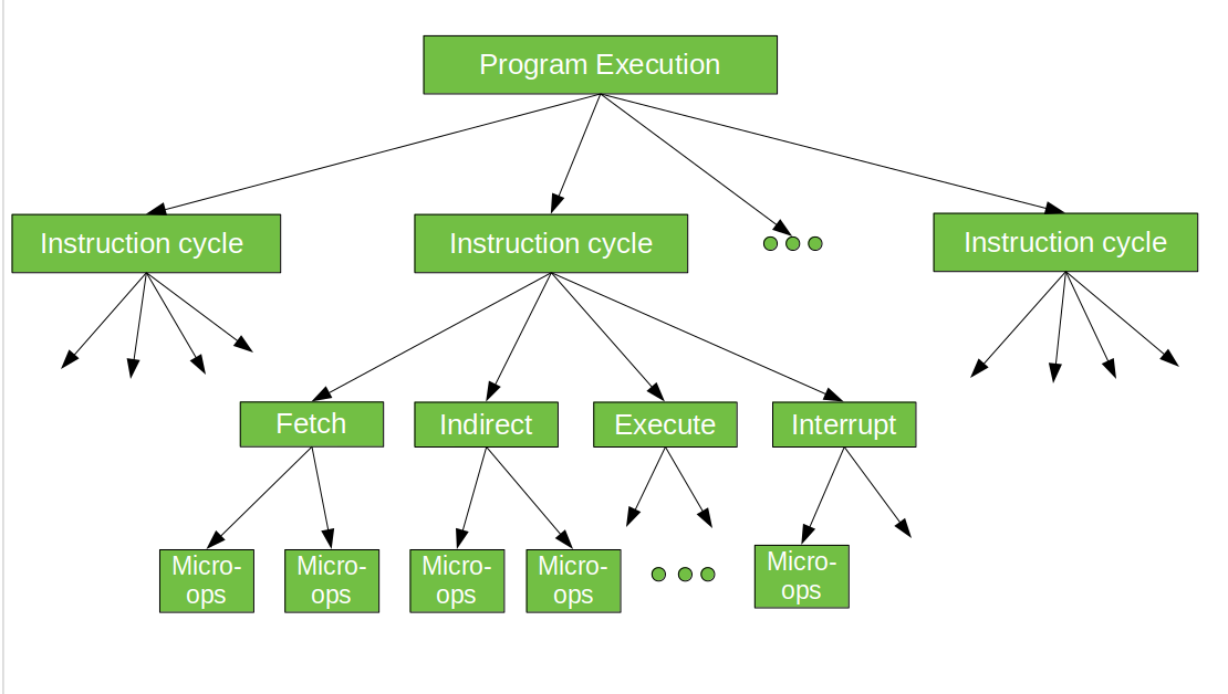
In computer central processing units, micro-operations (also known as micro-ops) are the functional or atomic, operations of a processor. These are low level instructions used in some designs to implement complex machine instructions. They generally perform operations on data stored in one or more registers. They transfer data between registers or between external buses of the CPU, also performs arithmetic and logical operations on registers.
In executing a program, operation of a computer consists of a sequence of instruction cycles, with one machine instruction per cycle. Each instruction cycle is made up of a number of smaller units – Fetch, Indirect, Execute and Interrupt cycles. Each of these cycles involves series of steps, each of which involves the processor registers. These steps are referred as micro-operations. the prefix micro refers to the fact that each of the step is very simple and accomplishes very little. Figure below depicts the concept being discussed here.
RISC and CISC
Reduced Instruction Set Architecture (RISC) –
The main idea behind is to make hardware simpler by using an instruction set composed of a few basic steps for loading, evaluating, and storing operations just like a load command will load data, store command will store the data.
Complex Instruction Set Architecture (CISC) –
The main idea is that a single instruction will do all loading, evaluating, and storing operations just like a multiplication command will do stuff like loading data, evaluating, and storing it, hence it’s complex.
RISC: Reduce the cycles per instruction at the cost of the number of instructions per program.
CISC: The CISC approach attempts to minimize the number of instructions per program but at the cost of increase in number of cycles per instruction.
Earlier when programming was done using assembly language, a need was felt to make instruction do more tasks because programming in assembly was tedious and error-prone due to which CISC architecture evolved but with the uprise of high-level language dependency on assembly reduced RISC architecture prevailed.
Characteristic of RISC –
Simpler instruction, hence simple instruction decoding.
Instruction comes undersize of one word.
Instruction takes a single clock cycle to get executed.
More general-purpose registers.
Simple Addressing Modes.
Less Data types.
Pipeline can be achieved.
Characteristic of CISC –
Complex instruction, hence complex instruction decoding.
Instructions are larger than one-word size.
Instruction may take more than a single clock cycle to get executed.
Less number of general-purpose registers as operation get performed in memory itself.
Complex Addressing Modes.
More Data types.
RISCCISCFocus on software Focus on hardware
Uses only Hardwired control unit Uses both hardwired and micro programmed control unit
Transistors are used for more registers Transistors are used for storing complex
Instructions
Fixed sized instructions Variable sized instructions
Can perform only Register to Register Arithmetic operations Can perform REG to REG or REG to MEM or MEM to MEM
Requires more number of registers Requires less number of registers
Code size is large Code size is small
An instruction execute in a single clock cycle Instruction takes more than one clock cycle
An instruction fit in one word Instructions are larger than the size of one word
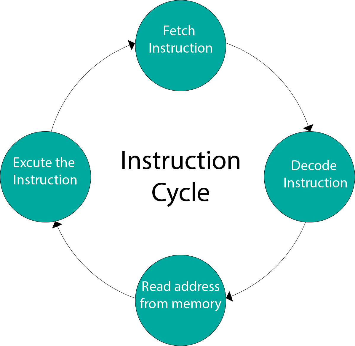
Instruction Cycle
A program residing in the memory unit of a computer consists of a sequence of instructions. These instructions are executed by the processor by going through a cycle for each instruction.
In a basic computer, each instruction cycle consists of the following phases:
Fetch instruction from memory.
Decode the instruction.
Read the effective address from memory.
Execute the instruction.
Input-Output Configuration
In computer architecture, input-output devices act as an interface between the machine and the user.
Instructions and data stored in the memory must come from some input device. The results are displayed to the user through some output device.
The following block diagram shows the input-output configuration for a basic computer.
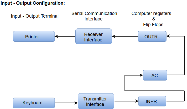
The input-output terminals send and receive information.
The amount of information transferred will always have eight bits of an alphanumeric code.
The information generated through the keyboard is shifted into an input register 'INPR'.
The information for the printer is stored in the output register 'OUTR'.
Registers INPR and OUTR communicate with a communication interface serially and with the AC in parallel.
The transmitter interface receives information from the keyboard and transmits it to INPR.
The receiver interface receives information from OUTR and sends it to the printer serially.
Single Bus Structure and Double Bus Structure
1. Single Bus Structure :
In single bus structure, one common bus used to communicate between peripherals and microprocessor. It has disadvantages due to use of one common bus.
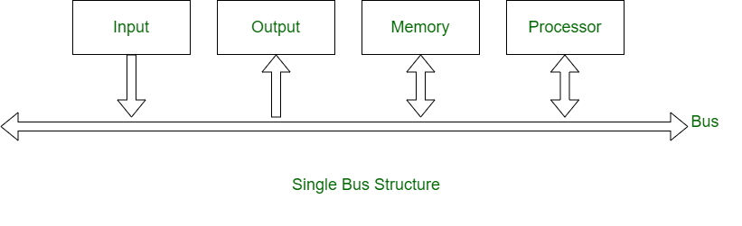
2. Double Bus Structure :
In double bus structure, one bus is used to fetch instruction while other is used to fetch data, required for execution. It is to overcome the bottleneck of single bus structure.
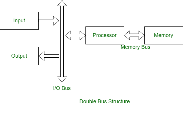
Differences between Single Bus and Double Bus Structure :
Single Bus StructureDouble Bus StructureOne common bus is used for communication between peripherals and processor. Two buses are used, one for communication from peripherals and other for processor.
Instructions and data both are transferred in same bus. Instructions and data both are transferred in different buses.
Its performance is low. Its performance is high.
Cost of single bus structure is low. Cost of double bus structure is high.
Number of cycles for execution is more. Number of cycles for execution is less.
Execution of process is slow. Execution of process is fast.
Number of registers associated are less. Number of registers associated are more.
At a time single operand can be read from bus. At a time two operands can be read.
Three-Bus Organization I
n a three-bus organization, two buses may be used as source buses while the third is used as destination. The source buses move data out of registers (out-bus), and the destination bus may move data into a register (in-bus). Each of the two outbuses is connected to an ALU input point. The output of the ALU is connected directly to the in-bus. As can be expected, the more buses we have, the more data we can move within a single clock cycle. However, increasing the number of buses will also increase the complexity of the hardware. Figure (8.3) shows an example of a three-bus datapath.
Branch Instruction
A branch is an instruction in a computer program that can cause a computer to begin executing a different instruction sequence and thus deviate from its default behaviour of executing instructions in order. Branch may also refer to the act of switching execution to a different instruction sequence as a result of executing a branch instruction. Branch instructions are used to implement control flow in program loops and conditionals (i.e., executing a particular sequence of instructions only if certain conditions are satisfied).
A branch instruction can be either an unconditional branch, which always results in branching or a conditional branch, which may or may not cause branching depending on some condition. Also, depending on how it specifies the address of the new instruction sequence (the target address).
A branch instruction is generally classified as direct, indirect or relative. It means the instruction contains the target address, specifies where the target address is to be found (e.g., a register or memory location), or specifies the difference between the current and target addresses. A branch instruction computes the target address in one of four ways:
A target address is the sum of a constant and the address of the branch instruction itself.
The target address is the absolute address given as an operand to the instruction.
The target address is the address found in the Link Register.
The target address is the address found in Count Register.
Hardwired v/s Micro-programmed Control Unit
Hardwired Control Unit –
The control hardware can be viewed as a state machine that changes from one state to another in every clock cycle, depending on the contents of the instruction register, the condition codes and the external inputs. The outputs of the state machine are the control signals. The sequence of the operation carried out by this machine is determined by the wiring of the logic elements and hence named as “hardwired”.
Fixed logic circuits that correspond directly to the Boolean expressions are used to generate the control signals.
Hardwired control is faster than micro-programmed control.
A controller that uses this approach can operate at high speed.
RISC architecture is based on hardwired control unit
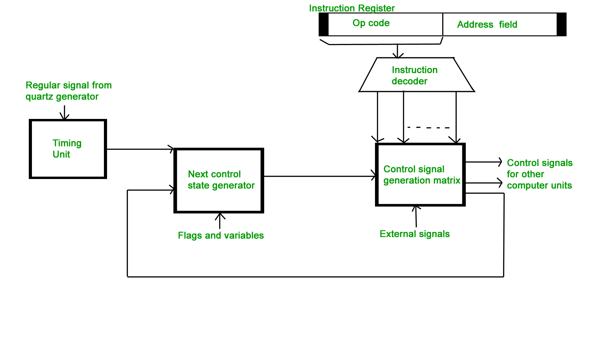
Micro-programmed Control Unit –
The control signals associated with operations are stored in special memory units inaccessible by the programmer as Control Words.
Control signals are generated by a program are similar to machine language programs.
Micro-programmed control unit is slower in speed because of the time it takes to fetch microinstructions from the control memory.
Some Important Terms –
Control Word : A control word is a word whose individual bits represent various control signals.
Micro-routine : A sequence of control words corresponding to the control sequence of a machine instruction constitutes the micro-routine for that instruction.
Micro-instruction : Individual control words in this micro-routine are referred to as microinstructions.
Micro-program : A sequence of micro-instructions is called a micro-program, which is stored in a ROM or RAM called a Control Memory (CM).
Control Store : the micro-routines for all instructions in the instruction set of a computer are stored in a special memory called the Control Store.
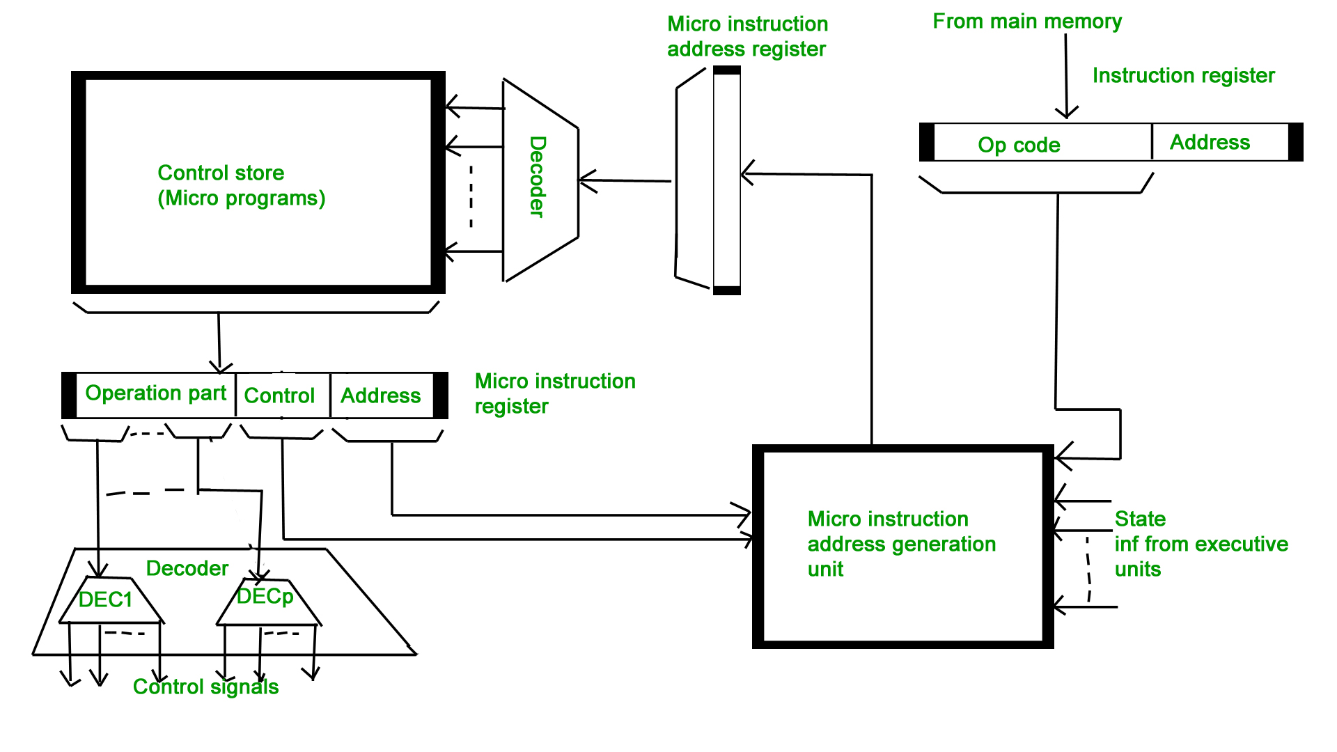
Types of Micro-programmed Control Unit – Based on the type of Control Word stored in the Control Memory (CM), it is classified into two types :
1. Horizontal Micro-programmed control Unit :
The control signals are represented in the decoded binary format that is 1 bit/CS. Example: If 53 Control signals are present in the processor than 53 bits are required. More than 1 control signal can be enabled at a time.
It supports longer control word.
It is used in parallel processing applications.
It allows higher degree of parallelism. If degree is n, n CS are enabled at a time.
It requires no additional hardware(decoders). It means it is faster than Vertical Microprogrammed.
It is more flexible than vertical microprogrammed
2. Vertical Micro-programmed control Unit :
The control signals re represented in the encoded binary format. For N control signals- Log2(N) bits are required.
It supports shorter control words.
It supports easy implementation of new control signals therefore it is more flexible.
It allows low degree of parallelism i.e., degree of parallelism is either 0 or 1.
Requires an additional hardware (decoders) to generate control signals, it implies it is slower than horizontal microprogrammed.
It is less flexible than horizontal but more flexible than that of hardwired control unit.
UNIT 3
The key characteristics of memory devices or memory system are as follows:
Location
Capacity
Unit of Transfer
Access Method
Performance
Physical type
Physical characteristics
Organization
1. Location:
It deals with the location of the memory device in the computer system. There are three possible locations:
CPU : This is often in the form of CPU registers and small amount of cache
Internal or main: This is the main memory like RAM or ROM. The CPU can directly access the main memory.
External or secondary: It comprises of secondary storage devices like hard disks, magnetic tapes. The CPU doesn’t access these devices directly. It uses device controllers to access secondary storage devices.
2. Capacity:
The capacity of any memory device is expressed in terms of: i)word size ii)Number of words
Word size: Words are expressed in bytes (8 bits). A word can however mean any number of bytes. Commonly used word sizes are 1 byte (8 bits), 2bytes (16 bits) and 4 bytes (32 bits).
Number of words: This specifies the number of words available in the particular memory device. For example, if a memory device is given as 4K x 16.This means the device has a word size of 16 bits and a total of 4096(4K) words in memory.
3. Unit of Transfer:
It is the maximum number of bits that can be read or written into the memory at a time. In case of main memory, it is mostly equal to word size. In case of external memory, unit of transfer is not limited to the word size; it is often larger and is referred to as blocks.
4. Access Methods:
It is a fundamental characteristic of memory devices. It is the sequence or order in which memory can be accessed. There are three types of access methods:
Random Access: If storage locations in a particular memory device can be accessed in any order and access time is independent of the memory location being accessed. Such memory devices are said to have a random access mechanism. RAM (Random Access Memory) IC’s use this access method.
Serial Access: If memory locations can be accessed only in a certain predetermined sequence, this access method is called serial access. Magnetic Tapes, CD-ROMs employ serial access methods.
Semi random Access: Memory devices such as Magnetic Hard disks use this access method. Here each track has a read/write head thus each track can be accessed randomly but access within each track is restricted to a serial access.
5. Performance: The performance of the memory system is determined using three parameters
Access Time: In random access memories, it is the time taken by memory to complete the read/write operation from the instant that an address is sent to the memory. For non-random access memories, it is the time taken to position the read write head at the desired location. Access time is widely used to measure performance of memory devices.
Memory cycle time: It is defined only for Random Access Memories and is the sum of the access time and the additional time required before the second access can commence.
Transfer rate: It is defined as the rate at which data can be transferred into or out of a memory unit.
6. Physical type: Memory devices can be either semiconductor memory (like RAM) or magnetic surface memory (like Hard disks).
7.Physical Characteristics:
Volatile/Non- Volatile: If a memory devices continues hold data even if power is turned off. The memory device is non-volatile else it is volatile.
8. Organization:
Erasable/Non-erasable: The memories in which data once programmed cannot be erased are called Non-erasable memories. Memory devices in which data in the memory can be erased is called erasable memory.
E.g. RAM(erasable), ROM(non-erasable).
Main Memory
The main memory acts as the central storage unit in a computer system. It is a relatively large and fast memory which is used to store programs and data during the run time operations.
The primary technology used for the main memory is based on semiconductor integrated circuits. The integrated circuits for the main memory are classified into two major units.
RAM (Random Access Memory) integrated circuit chips
ROM (Read Only Memory) integrated circuit chips
RAM integrated circuit chips
The RAM integrated circuit chips are further classified into two possible operating modes, static and dynamic.
The primary compositions of a static RAM are flip-flops that store the binary information. The nature of the stored information is volatile, i.e. it remains valid as long as power is applied to the system. The static RAM is easy to use and takes less time performing read and write operations as compared to dynamic RAM.
The dynamic RAM exhibits the binary information in the form of electric charges that are applied to capacitors. The capacitors are integrated inside the chip by MOS transistors. The dynamic RAM consumes less power and provides large storage capacity in a single memory chip.
RAM chips are available in a variety of sizes and are used as per the system requirement. The following block diagram demonstrates the chip interconnection in a 128 * 8 RAM chip.
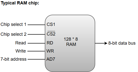
A 128 * 8 RAM chip has a memory capacity of 128 words of eight bits (one byte) per word. This requires a 7-bit address and an 8-bit bidirectional data bus.
The 8-bit bidirectional data bus allows the transfer of data either from memory to CPU during a read operation or from CPU to memory during a write operation.
The read and write inputs specify the memory operation, and the two chip select (CS) control inputs are for enabling the chip only when the microprocessor selects it.
The bidirectional data bus is constructed using three-state buffers.
The output generated by three-state buffers can be placed in one of the three possible states which include a signal equivalent to logic 1, a signal equal to logic 0, or a high-impedance state.
Note: The logic 1 and 0 are standard digital signals whereas the high-impedance state behaves like an open circuit, which means that the output does not carry a signal and has no logic significance.
The following function table specifies the operations of a 128 * 8 RAM chip.
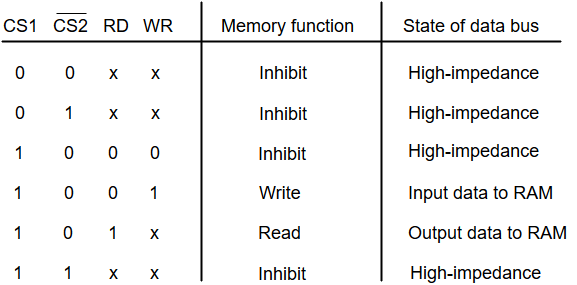
From the functional table, we can conclude that the unit is in operation only when CS1 = 1 and CS2 = 0. The bar on top of the second select variable indicates that this input is enabled when it is equal to 0.
ROM integrated circuit
The primary component of the main memory is RAM integrated circuit chips, but a portion of memory may be constructed with ROM chips.
A ROM memory is used for keeping programs and data that are permanently resident in the computer.
Apart from the permanent storage of data, the ROM portion of main memory is needed for storing an initial program called a bootstrap loader. The primary function of the bootstrap loader program is to start the computer software operating when power is turned on.
ROM chips are also available in a variety of sizes and are also used as per the system requirement. The following block diagram demonstrates the chip interconnection in a 512 * 8 ROM chip.
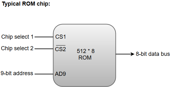
A ROM chip has a similar organization as a RAM chip. However, a ROM can only perform read operation; the data bus can only operate in an output mode.
The 9-bit address lines in the ROM chip specify any one of the 512 bytes stored in it.
The value for chip select 1 and chip select 2 must be 1 and 0 for the unit to operate. Otherwise, the data bus is said to be in a high-impedance state.
Memory system considerations
Speed
Cost
Size of chip
Power dissipation
Memory controller
Refresh Overhead
Used Between processor and memory
The Memory Subsystem
Except for the CPU, the most important subsystem in the computer
all von Neumann digital computers have memory
modern systems have multiple, independent memories
often on-chip ... our 'C31 CPU has two small on-chip SRAMs
Do not confuse the addressable memory space with the actual memory subsystem
number of bits in processor-generated address can be more (or less) than number of bits used to address physical memory
some setups have holes in memory, others have MMUs (i.e. memory management units)
SRAM
Static Random Access Memory
essentially a combinational table look-up (also writable)
easiest type of memory to use
fast, often rather expensive, large high pinout packages
Logic symbol needs:
1 wire for requesting a read (aka OE)
m wires for the data 1 wire for requesting a write (aka WE)
n wires for addressing 2n cells usually a chip select (1 wire)
So-called “separate I/O” variant exists too
a second m-wide data path (separate dedicated paths for reading and for writing)
DRAM
Dynamic Random Access Memory
data stored as charge on a tiny capacitor (MOSFET-gate)
organized in rows and columns, addressed separately & sequentially
not the same as SDRAM (synchronous DRAM)
Logic symbol needs:
1 wire for enabling data outputs (aka OE), often omitted
1 wire for requesting a write (aka WE)
m wires for the data
n/2 wires for addressing 2n cells (second generation)
2 wires for row vs column address select
often a chip select (1 wire) Capacity: high
Speed (fast, but not as fast as SRAM due to more complex cycle)
Cost (relatively inexpensive)
Cache Memory
Cache Memory is a special very high-speed memory. It is used to speed up and synchronizing with high-speed CPU. Cache memory is costlier than main memory or disk memory but economical than CPU registers. Cache memory is an extremely fast memory type that acts as a buffer between RAM and the CPU. It holds frequently requested data and instructions so that they are immediately available to the CPU when needed.
Cache memory is used to reduce the average time to access data from the Main memory. The cache is a smaller and faster memory which stores copies of the data from frequently used main memory locations. There are various different independent caches in a CPU, which store instructions and data.
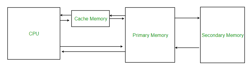
Levels of memory:
Level 1 or Register –
It is a type of memory in which data is stored and accepted that are immediately stored in CPU. Most commonly used register is accumulator, Program counter, address register etc.
Level 2 or Cache memory –
It is the fastest memory which has faster access time where data is temporarily stored for faster access.
Level 3 or Main Memory –
It is memory on which computer works currently. It is small in size and once power is off data no longer stays in this memory.
Level 4 or Secondary Memory –
It is external memory which is not as fast as main memory but data stays permanently in this memory.
Cache Performance:
When the processor needs to read or write a location in main memory, it first checks for a corresponding entry in the cache.
If the processor finds that the memory location is in the cache, a cache hit has occurred and data is read from cache
If the processor does not find the memory location in the cache, a cache miss has occurred. For a cache miss, the cache allocates a new entry and copies in data from main memory, then the request is fulfilled from the contents of the cache.
The performance of cache memory is frequently measured in terms of a quantity called Hit ratio.Hit ratio = hit / (hit + miss) = no. of hits/total accesses
We can improve Cache performance using higher cache block size, higher associativity, reduce miss rate, reduce miss penalty, and reduce the time to hit in the cache.
Main Memory
he main memory acts as the central storage unit in a computer system. It is a relatively large and fast memory which is used to store programs and data during the run time operations.
The primary technology used for the main memory is based on semiconductor integrated circuits. The integrated circuits for the main memory are classified into two major units.
RAM (Random Access Memory) integrated circuit chips
ROM (Read Only Memory) integrated circuit chips
Memory Hierarchy or Memory structure
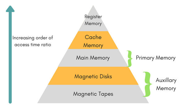
Elements of cache design
There are a few basic design elements that serve to classify and differentiate cache architectures. They are listed down:
Cache Addresses
Cache Size
Mapping Function
Replacement Algorithm
Write Policy
Line Size
Number of caches
1. Cache Addresses
When virtual addresses are used, the cache can be placed between the processor and the MMU or between the MMU and main memory. A logical cache, also known as a virtual cache, stores data using virtual addresses. The processor accesses the cache directly, without going through the MMU. This organization is shown in Figure 3.

A physical cache stores data using main memory physical addresses. This organization is shown in Figure 4. One advantage of the logical cache is that cache access speed is faster than for a physical cache, because the cache can respond before the MMU performs an address translation.

2. Cache Size:
The size of the cache should be small enough so that the overall average cost per bit is close to that of main memory alone and large enough so that the overall average access time is close to that of the cache alone.
3. Mapping Function:
As there are fewer cache lines than main memory blocks, an algorithm is needed for mapping main memory blocks into cache lines. Further, a means is needed for determining which main memory block currently occupies a cache line. The choice of the mapping function dictates how the cache is organized. Three techniques can be used: direct, associative, and set associative.
DIRECT MAPPING: The simplest technique, known as direct mapping, maps each block of main memory into only one possible cache line.
The direct mapping technique is simple and inexpensive to implement.
ASSOCIATIVE MAPPING: Associative mapping overcomes the disadvantage of direct mapping by permitting each main memory block to be loaded into any line of the cache
SET-ASSOCIATIVE MAPPING: Set-associative mapping is a compromise that exhibits the strengths of both the direct and associative approaches. With set-associative mapping, block can be mapped into any of the lines of set j.
4. Replacement Algorithms:
Once the cache has been filled, when a new block is brought into the cache, one of the existing blocks must be replaced. For direct mapping, there is only one possible line for any particular block, and no choice is possible. For the associative and set associative techniques, a replacement algorithm is needed. To achieve high speed, such an algorithm must be implemented in hardware. Least Recently Used (LRU), Least Frequently Used(LFU), First In First Out (FIFO) are some replacement algorithms.
5. Write Policy
When a block that is resident in the cache is to be replaced, there are two cases to consider. If the old block in the cache has not been altered, then it may be overwritten with a new block without first writing out the old block. If at least one write operation has been performed on a word in that line of the cache, then main memory must be updated by writing the line of cache out to the block of memory before bringing in the new block.
The simplest policy is called write through. Using this technique, all write operations are made to main memory as well as to the cache, ensuring that main memory is always valid. An alternative technique, known as write back, minimizes memory writes. With write back, updates are made only in the cache. When an update occurs, a dirty bit, or use bit, associated with the line is set. Then, when a block is replaced, it is written back to main memory if and only if the dirty bit is set.
6. Line Size
Another design element is the line size. When a block of data is retrieved and placed in the cache, not only the desired word but also some number of adjacent words is retrieved. Basically, as the block size increases, more useful data are brought into the cache. The hit ratio will begin to decrease, however, as the block becomes even bigger and the probability of using the newly fetched information becomes less than the probability of reusing the information that has to be replaced.
The relationship between block size and hit ratio is complex, depending on the locality characteristics of a particular program, and no definitive optimum value is found as of yet.
7.Number of Caches
When caches were originally introduced, the typical system had a single cache. More recently, the use of multiple caches has become an important aspect. There are two design issues surrounding number of caches.
MULTILEVEL CACHES: Most contemporary designs include both on-chip and external caches. The simplest such organization is known as a two-level cache, with the internal cache designated as level 1 (L1) and the external cache designated as level 2 (L2). There can also be 3 or more levels of cache. This helps in reducing main memory accesses.
UNIFIED VERSUS SPLIT CACHES: Earlier on-chip cache designs consisted of a single cache used to store references to both data and instructions. This is the unified approach. More recently, it has become common to split the cache into two: one dedicated to instructions and one dedicated to data. These two caches both exist at the same level. This is the split cache. Using a unified cache or a split cache is another design issue.
External memory
Eternal memory can also be known as secondary memory or backing store. It is used to store a huge amount of data because it has a huge capacity. At present, it can measure the data in hundreds of megabytes or even in gigabytes. The important property of external memory is that whenever the computer switches off, then stored information will not be lost. The external memory can be categorized into four parts:
Magnetic disk
Raid
Optical memory
Magnetic Tape
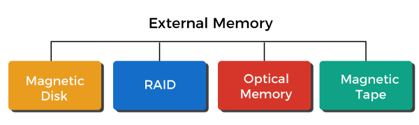
Magnetic Disks
A disk is a type of circular platter constructed by a nonmagnetic material, which is known as a substrate. It is covered with a magnetic coating used to hold the information. The substrate is traditionally constructed by aluminium or aluminium alloy material. But recently, another material has been introduced, which is known as glass substrates. There are various benefits of glass substrates, which are described as follows:
It has the ability to increase disk reliability by improving the uniformity of a magnetic film surface.
It is used to reduce the errors of read-write by doing a significant reduction in overall surface defects.
It has better stiffness, which will help to reduce disk dynamics. It has the great ability that it can withstand against shock and damage.
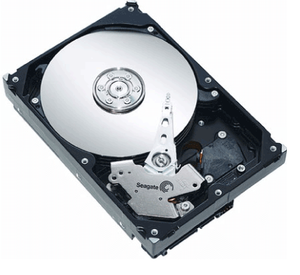
Magnetic Read and Write Memory
The most important component of external memory is still magnetic disks. Many systems, such as supercomputers, personal computers, and mainframes computers, contain both removable and fixed hard disks. We can conduct a coil named as the head so that we can recover the data on and later and then retrieve it from the disk. A lot of systems contain two heads that are read head and write head. While the operation of reading and writing, the platter is rotating while the head is stationary.
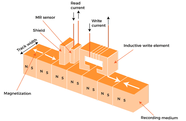
If the electricity is flowing through the coil, the write mechanism will exploit the fact that the coil will generate a magnetic field. The write head will receive the electric pulses, and the below surface will record the resulting magnetic pattern. It will be recorded into different patterns for negative and positive currents. If the electricity is flowing through the coil, the read mechanism will exploit the fact that it will generate an electric current in the coil. When the disk's surface passes under the head, it will produce a current with the same polarity as the already recorded one.
In this case, the structure of head is the same for reading and writing. Therefore, we can use the same head for both. These types of single heads can be used in older rigid disk systems and in floppy disk systems. A type of partially shielded magneto-resistive (MR) sensor consists in the read head. The electric resistance is contained in the MR material, which depends on the direction of magnetization of the medium moving under it.
Data Organization and formatting
The head is known as a small device, which is able to read from or write to the portion of the platter rotating beneath it. The width of each track is the same as head. We have thousands of tracks per surface. The gaps are used to show the separation of adjacent tracks. This can prevent or minimize the error which is generated because of the interference of magnetic fields or misalignment of the head. The sectors are used to transfer the data from and to the disks.
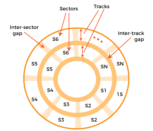
The fixed-length sectors will be used in the most contemporary systems with 512 bytes, which is nearly a universal sector size. Intersector gaps separate the adjacent sectors so that we can avoid imposing unreasonable precision requirements on the systems. At the same rate, we can scan the information with the help of rotating the disk at a fixed speed, which is called constant angular velocity (CAV).
There are various things in which disks can be divided. So it can divide into a series of concentric tracks and into a number of pie-shaped sectors. The CAV has an advantage in that the tracks and sectors are able to directly address the data with the help of CAV. The CAV also has a disadvantage in that the amount of data that is stored on the short inner tracks and the long outer tracks are the same.
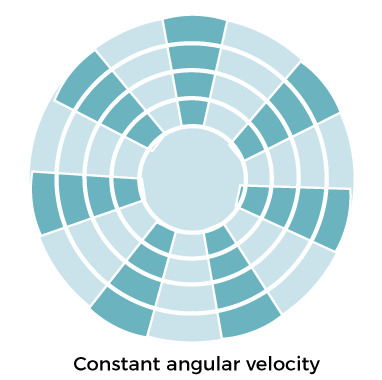
The modern hard disks introduce a technique to increase the density, which is called Multiple zone recording. Using this technique, the surface is able to divide into a number of concentric zones, which is typically equal to 16, which means 16 zones. The number of bits per track is constant within a zone. The zones which are closer to the centre have fewer amounts of bits or sectors as compared to the zones which are farther from the centre.

Physical characteristics
If there is a fixed head disk, then it will contain one read-write head per track. All of these heads are mounted on a rigid arm, which has the ability to extend across all tracks. If there is a movable head disk, then it will contain only one read-write head. Here the head is also mounted on the arm. The head can position above any track. Due to this purpose, the arm can be retracted or extended.
The disk drive always or permanently contains a non-removable disk. For example, in the personal computer, the hard disk can never be removed, or we can say that it is a non-removable disk. The removable disk is a type of disk that can be removed and replaced with other disks. Both sides of the platter contain the magnetizable coating for most of the disks, which will also be referred to as the double side. The single side disks are used in some less expensive disk systems.

A movable head is employed by the multiple platter disks with one head of read-write per platter surface. Form the centre of the disk, all the heads contain the same distance and move together because all the heads are mechanically fixed. In the platter, a set of all tracks in the same relative position will be known as a cylinder.
This type of mechanism is mostly used in a floppy disk. This type of disk is the least expensive, small, also contains a flexible platter. The sealed drive assemblies are almost free of contaminants, and it contains the Winchester's heads. IBM uses the term Winchester as a code name and it was used for the 3340 disk model prior to its announcement in IBM. The workstations and personal computers commonly contain a built-in disk, which is known as Winchester disk. This disk is also referred to as a hard disk.
On a movable system, there will be a seek time which can be defined as the time taken to position the head at the track. There will also be a rotation latency or rotation delay, which can be defined as the time taken from the starting of the sector to reach the head. The time it takes to get into a position to write or read is known as access time which is equal to the sum of rotational delay and seeks time, if any.
Once the head gets its position, we are able to perform the read or write operation as the sector moves under the head. This process can be called the data transfer portion of the operation, and the time taken while transferring the data will be known as the transfer time.
RAID
The RAID is also known as a redundant array of independent disks. It is a type of data virtualization technology, which is used to combine components of multiple disks into a logical unit so that they can improve the performance or create redundancy. If there are multiple disks/drives, it will allow the employment of various techniques such as disk mirroring, parity, and disk striping. We cannot consider RAID as a replacement for data backup. If RAID is going through the critical data, it will be backed up to a logical set of disks or other physical disks. When we make a connection with RAID, we will normally use the following terms:
Striping: In this, data will be split between more than one disk.
Optical Memory
The optical memory was released in 1982, and Sony and Philips developed it. These memories perform their operations with the help of light beams, and it also needs option drive for the operations. We can use optical memory to store backup, audio, video, and also for caring data. The speed of a flash drive and the hard drive is faster as compared to the read/write speed. There are various examples of optical memory that are Compact disk (CD), Bluray Disk (BD), and Digital Versatile Disk (DVD).
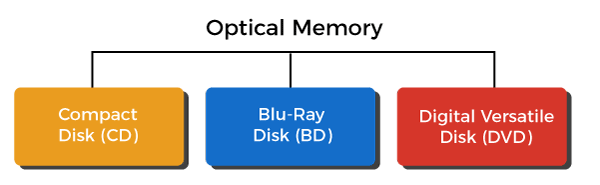
Compact Disk (CD)
It is a type of digital audio system, which is used to store data. It is composed of circular plastic, in which aluminium alloy is used to coat the single side of plastic, which is used to store the data. It also contains an additional thin plastic covering, which is used to protect the data. CD will perform its operations with the help of a CD drive. The compact disk can be called the non-erasable disk. Here we use the laser beam to imprint the data on the disk. In the starting, the CDs are used to hold the 60 to 75 minutes of audio information that has the ability to store about 700MB of data. But now, it can store 60 minutes of audio information on a single side. Now many devices have been developed which contains low cost and high capacity as compared to the CD.

Types of Compact Disk
CD-ROM:
CD-ROM is also known as CD read-only memory. It is mainly used to store computer data. As we know earlier, the compact disks were used to store the video and audio data, but it uses the digital form to store the data, so we can also be used the compact disks to store the computer data.
If there is some error in the audio and video appliance, it will ignore that error, and that error does not reflect in the produced video and audio. But if the computer data contains any error, then CD-ROM will not tolerate it, and that error will reflect in the produced data. At the time of indenting pills on the compact disks, it is impossible to prevent physical imperfection. So in order to detect and correct the error, we have to add some extra bits.
The compact disk (CD) and compact disk read-only memory (CD-ROM) contain one spiral track, beginning from the track's centre and spiral out towards the outer edge. CD-ROM uses the blocks or sectors to store the data. On the basis of tracks, the number of sectors varies. The inner tracks of the compact disk contain fewer sectors, and the outer track of the compact disk contains more sectors. The length of the sectors at the inner edge and the outer edge of disk is the same.
When the disk is rotating, the low power laser beam will be used to scan the sectors at the same rate. There can be a variation in the rotating speed of disk. If we are trying to access the sectors which are near to the centre of the disk, the disk will be rotated comparatively faster. If the sectors are present near the outer edge, the disk will be rotated slower as compared to the sectors near to centre of the disk.
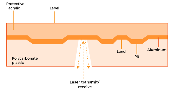
CD-R:
CD-R is also known as CD-Recordable. It is a type of write once read many, or we can say that it allows single time recording on a disk. It is used in these types of applications that require one or a small number of copies of a set of data. CD recordable composed of polycarbonate plastic substrate, coating of thin reflective metal, and a protective outer coating. Between the metal layers and the polycarbonate, there is a layer of organic polymer dye, which serves as a recording medium. With the help of dye, the reflectivity can be changed. When there is exposure to a specific frequency of light, the dye will be permanently transformed. The high-intensity laser is used to activate the dye. In the dye, marks are created by the laser that is used to mimic the reflective properties of lands (highest area) and pills (lower area) of the traditional CD.

CD-RW:
CD-RW is also known as CD-Rewritable. It is a type of compact disk format which allow us to repeatedly recording on a disk. CD rewritable and CD recordable both are composed of the same material. So it is also composed of polycarbonate plastic substrate, coating of thin reflective metal, and a protective outer coating. The dye will be replaced by an alloy in the CD-RW. When the alloy is heated and cooled down, then it will show some interesting behavior.
If there is a melting point and the alloy is heated above that point and cooled down, in this case, it will turn into a state which is known as the amorphous state, which is used to absorb light. If there is a case in which alloy is heated at 200o C and that temperature is maintained for a certain period, then a process known as annealing will occur, and it will turn alloy into the crystalline state.
The area of non-crystalline and crystalline will be formed with the help of controlling the temperature of a laser. The crystalline area is used to reflect the laser, while the other area is used to absorb it. These differences will be registered as digital data. We can further use the annealing process to delete the stored data. There is an advantage of CR-RW over CD-R and CD-ROM, i.e., we can rewrite the CD-RW, and after that, we can use it as true secondary storage.
Digital Versatile Disk (DVD)
The DVD (digital versatile disk) technology was first launched in 1996. The appearance of the CD (compact disk) and the DVD (digital versatile disk) has the same. The storage size is the main difference between CD and DVD. So the storage size of a DVD is much larger than the CD. While designing DVDs, there are several changes that are done in their design to make the storage larger.
DVD uses the shorter wavelength of a laser beam to imprint the data than the CDs laser beam wavelength. With the help of a shorter laser beam wavelength, the lights are able to focus on a small spot. Pits of CDs are much larger than the pits of DVDs. The tracks on DVD is placed very close than the tracks on a CD. By doing all the changes in the design of a DVD, it has a 4.7GB storage size. We can more increase the storage capability by using the two-sided disk and two-layered disk.

Two Layered Disk
The first base of the two-layered disk is the same as CD that means it is also composed of circular plastic. But in this disk, we use translucent material rather than aluminium to cover the lands and pits of the first base. This material is able to solve the purpose of a reflector. The program of a translucent layer is doing in a way that it can store the data with the help of indenting pits onto it. The second layer of lands and pits contains the reflective material. In order to retrieve the binary pattern, when the laser beam is focused on the first layer, then sufficient light will be reflected by the translucent material, which will be captured by the detector. After that, the second layer will reflect a small light, and that light is a noise. That's why it will be cancelled by the detector.
Similarly, the focus of a laser is on the second layer and wants to read it, the first layer will reflect a small light, and that light will be cancelled with the help of detector.
Two-Sided Disk
In a two-sided disk, the implementation of tracks will be applied on both sides of the DVDs. This structure is also known as two single-sided disks. These disks will be put together so that they can form a sandwich. But the topmost disk will be turned upside down.
Blu-Ray DVD
A Blu-ray disk is a type of high capacity optical disk medium, which is used to store a huge amount of data and to record and playback high definition video. Blu-ray was designed to supersede the DVD. While a CD is able to store 700 MB of data and a DVD is able to store 4.7 GB of data, a single Blu-ray disk is able to store up to 25 GB of data. The dual-layer Blu-ray disks can hold 50 GB of data. That amount of storage is equivalent to 4 hours of HDTV. There is also a double-sided dual-layer DVD, which is commonly used and able to store 17 GB of data.
Blu-ray disk uses the blue lasers, which help them to hold more information as compared to other optical media. The laser is actually known as 'blue-violet', but the developer rolls off the tongue to make 'Blue-violet-ray' a little earlier as 'Blu-ray'. The CDs and DVDs use the red laser, and their wavelength (650 nm) is greater than the blue-violet laser (405nm). With the help of a small wavelength, the laser can focus on a small area. In Blu-ray disks, we can use the same size, which is used by CD or DVD and store a large amount of data on a disk. Blu-ray is able to provide very high resolution as compared to the DVD. On the basis of standard definition, a DVD can provide a definition of 720x480 pixels. In contrast, the Blu-ray high definition contains 1920X1080 pixel resolution.

Magnetic Tape
Reading and writing techniques in the tape system is the same as the disk system. In this, the medium is flexible polyester tape coated with a magnetizable material. The tape's data can be structured as a number of parallel tracks that will be run lengthwise. In this form, the recording of data can be called a parallel recording. Instead of the parallel recording, most of the modern system uses serial recording. The serial recording uses the sequence of bits along with each track to lay of the data. It is done with the help of a magnetic disk. In the serial recoding, the disk contains the physical record on the tape, which can be described as the data which are read and write in the contiguous blocks.
The gaps are used to separate the blocks on the tape, which can also be known as inter-record gaps. With the disk, we format the tape so that we can assist in locating physical records. When the data are being recorded in the techniques of serial tape, we record the first set of bits along with the whole tape's length. When we reach the end of a tape, the head will be repositioned so that they can record a new track. This time, the tape will follow the opposite direction to again record its whole length. This process will be continued until the tape is full.
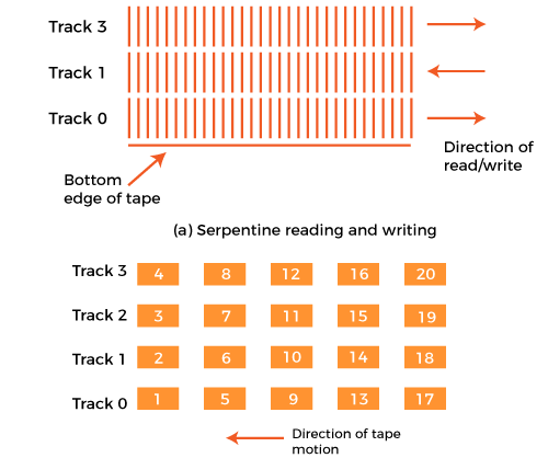
A tape drive can be accessed as a sequential access device. If the current position of the head is beyond the desired result, we have to rewind the tape at a certain distance and starting reading forward. During the operation of reading and writing only, the tape is in motion. The difference between tape and disk drive is that the disk drive can be referred to as a direct access device. A disk drive is able to get the desired result without sequentially reading all sectors on a disk. It has to only wait until the intervening sectors have arrived within one track. After that, it is able to successive access to any track.
The magnetic tape can also be known as a type of second memory. It can also be used as the slowest speed and lowest cost member of the memory hierarchy. There is also a linear tape technology, which is a type of cartridge system. It was developed in late the 1990s. In the market, the LTO can be described as an alternative to various properties systems..
Cache Memory in Computer Organization
Cache Memory is a special very high-speed memory. It is used to speed up and synchronizing with high-speed CPU. Cache memory is costlier than main memory or disk memory but economical than CPU registers. Cache memory is an extremely fast memory type that acts as a buffer between RAM and the CPU. It holds frequently requested data and instructions so that they are immediately available to the CPU when needed.
Cache memory is used to reduce the average time to access data from the Main memory. The cache is a smaller and faster memory which stores copies of the data from frequently used main memory locations. There are various different independent caches in a CPU, which store instructions and data.
UNIT 4
Input-Output Processor/Module
The DMA mode of data transfer reduces CPU’s overhead in handling I/O operations. It also allows parallelism in CPU and I/O operations. Such parallelism is necessary to avoid wastage of valuable CPU time while handling I/O devices whose speeds are much slower as compared to CPU. The concept of DMA operation can be extended to relieve the CPU further from getting involved with the execution of I/O operations. This gives rises to the development of special purpose processor called Input-Output Processor (IOP) or IO channel.
The Input Output Processor (IOP) is just like a CPU that handles the details of I/O operations. It is more equipped with facilities than those are available in typical DMA controller. The IOP can fetch and execute its own instructions that are specifically designed to characterize I/O transfers. In addition to the I/O – related tasks, it can perform other processing tasks like arithmetic, logic, branching and code translation. The main memory unit takes the pivotal role. It communicates with processor by the means of DMA.
The block diagram –
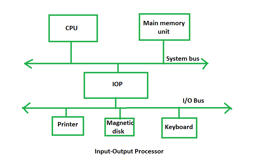
The Input Output Processor is a specialized processor which loads and stores data into memory along with the execution of I/O instructions. It acts as an interface between system and devices. It involves a sequence of events to executing I/O operations and then store the results into the memory.
Advantages –
The I/O devices can directly access the main memory without the intervention by the processor in I/O processor based systems.
It is used to address the problems that are arises in Direct memory access method.
Interrupt Driven I/O
Interrupt driven I/O is an alternative scheme dealing with I/O. Interrupt I/O is a way of controlling input/output activity whereby a peripheral or terminal that needs to make or receive a data transfer sends a signal. This will cause a program interrupt to be set. At a time appropriate to the priority level of the I/O interrupt. Relative to the total interrupt system, the processors enter an interrupt service routine. The function of the routine will depend upon the system of interrupt levels and priorities that is implemented in the processor. The interrupt technique requires more complex hardware and software, but makes far more efficient use of the computer’s time and capacities. Figure 2 shows the simple interrupt processing.

Figure 2: Simple Interrupt Processing
For input, the device interrupts the CPU when new data has arrived and is ready to be retrieved by the system processor. The actual actions to perform depend on whether the device uses I/O ports or memory mapping.
For output, the device delivers an interrupt either when it is ready to accept new data or to acknowledge a successful data transfer. Memory-mapped and DMA-capable devices usually generate interrupts to tell the system they are done with the buffer.
Here the CPU works on its given tasks continuously. When an input is available, such as when someone types a key on the keyboard, then the CPU is interrupted from its work to take care of the input data. The CPU can work continuously on a task without checking the input devices, allowing the devices themselves to interrupt it as necessary.
Basic Operations of Interrupt
CPU issues read command.
I/O module gets data from peripheral whilst CPU does other work.
I/O module interrupts CPU.
CPU requests data.
I/O module transfers data.
Interrupt Processing
A device driver initiates an I/O request on behalf of a process.
The device driver signals the I/O controller for the proper device, which initiates the requested I/O.
The device signals the I/O controller that is ready to retrieve input, the output is complete or that an error has been generated.
The CPU receives the interrupt signal on the interrupt-request line and transfer control over the interrupt handler routine.
The interrupt handler determines the cause of the interrupt, performs the necessary processing and executes a “return from” interrupt instruction.
The CPU returns to the execution state prior to the interrupt being signaled.
The CPU continues processing until the cycle begins again.

Advantages & Disadvantages of Interrupt Drive I/O
Advantages
- fast
- efficient
Disadvantages
- can be tricky to write if using a low level language
- can be tough to get various pieces to work well together
- usually done by the hardware manufacturer / OS maker, e.g. Microsoft
Design Issues
There are 2 main problems for interrupt I/O, which are:
There are multiple I/O modules, how should the processor determine the device that issued the interrupt signal?
How does the processor decide which module to process when multiple interrupts have occurred?
There are 4 main ways to counter these problems, which are:
Multiple Interrupt Lines
Software Poll
Daisy Chain (Hardware Poll, Vectored)
Bus Arbitration (Vectored)
COA-Priority Interrupt
In a typical application, a number of I/O devices are attached to computer, with each device being able to originate an interrupt request, so to provide services to device which initiate interrupt request, the task of interrupt system is to identify the source(device) of interrupt and then provide services to them.
But, in most cases there is a possibility that several sources will request service simultaneously.So, in this case, the interrupt system must also need to decide which device to service first.But, these simple interrupt system are not able for that, so, another system known as Priority interrupt system is provided.
Priority Interrupt are systems, that establishes a Priority over the various sources(interrupt devices) to determine which condition is to be serviced first when two or more requests arrive simultaneously.This system may also determine which condition are permitted to interrupt to the computer while another interrupt is being serviced.
Usually, in Priority Systems, higher-priority interrupt levels are served first, as if they delayed or interrupted, could have serious consequences.And the devices with high-speed transfer such as magnetic disks are given high-priority, and slow devices such as keyboards receives low-priority.
Establishing Priority of Simultaneous Interrupt:
The priority of simultaneous interrupts can be established either by software method or hardware.
The software method which gives priority to simultaneous interrupt is:
Polling
And the hardware method which gives priority to simultaneous interrupt is:
Daisy-Chaining Priority
Now, we will explore to each one of them one by one.
1. Polling:
Polling is the software method of establishing priority of simultaneous interrupt.In this method, when the processor detects an interrupt, it branches to an interrupt service routine whose job is to pull each I/O module to determine which module caused the interrupt.
The poll could be in the form of separate command line(e.g., Test I/O).In this case, the processor raises the Test I/O and places the address of particular I/O module on the address line.If it has interrupt that is, if interrupt is identified in it.
And, it is the order in which they are tested i.e., the order in which they appear on address line(Service Routine) determine the priority of each interrupt.As while testing, highest priority source(devices) are tested first then lower-priority devices.
This is very simple method of establishing priority on simultaneous interrupt.But the disadvantage of polling is that it is very time consuming.
2. Daisy-Chaining Priority:
The Daisy–Chaining method of establishing priority on interrupt sources uses the hardware i.e., it is the hardware means of establishing priority.
In this method, all the device, whether they are interrupt sources or not, connected in a serial manner.Means the device with highest priority is placed in the first position, which is followed by lowest priority device.And all device share a common interrupt request line, and the interrupt acknowledge line is daisy chained through the modules.
The figure shown below, this method of connection with three devices and the CPU.

It works as follows:
When any device raise an interrupt, the interrupt request line goes activated, the processor when sense it, it sends out an interrupt acknowledge which is first received by device1.If device1 does not need service, i.e., processor checks, whether the device has pending interrupt or initiate interrupt request, if the result is no, then the signal is passed to device2 by placing 1 in the PO(Priority Out) of device1.And if device need service then service is given to them by placing first 0 in the PO of device1, which indicate the next-lower-priority device that acknowledge signal has been blocked.And device that have processor responds by inserting its own interrupt vector address(VAD) into the data bus for the CPU to use during interrupt cycle.
In this way, it gave services to interrupt source according to their priority.And thus, we can say that, it is the order of device in chain that determine the priority of interrupt sources.
Interrupt Handling:
We know that instruction cycle consists of fetch, decode, execute and read/write functions. After every instruction cycle the processor will check for interrupts to be processed if there is no interrupt is present in the system it will go for the next instruction cycle which is given by the instruction register.
If there is an interrupt present then it will trigger the interrupt handler, the handler will stop the present instruction which is processing and save its configuration in a register and load the program counter of the interrupt from a location which is given by the interrupt vector table. After processing the interrupt by the processor interrupt handler will load the instruction and its configuration from the saved register, process will start its processing where it’s left. This saving the old instruction processing configuration and loading the new interrupt configuration is also called as context switching.
The interrupt handler is also called as Interrupt service routine (ISR). There are different types of interrupt handler which will handle different interrupts. For example for the clock in a system will have its interrupt handler, keyboard it will have its interrupt handler for every device it will have its interrupt handler.
The main features of the ISR are
Interrupts can occur at any time they are asynchronous. ISR’s can call for asynchronous interrupts.
Interrupt service mechanism can call the ISR’s from multiple sources.
ISR’s can handle both maskable and non maskable interrupts. An instruction in a program can disable or enable an interrupt handler call.
ISR on beginning of execution it will disable other devices interrupt services. After completion of the ISR execution it will re initialize the interrupt services.
The nested interrupts are allowed in ISR for diversion to other ISR.
Type of Interrupt Handlers:
First Level Interrupt Handler (FLIH) is hard interrupt handler or fast interrupt handler. These interrupt handlers have more jitter while process execution and they are mainly maskable interrupts
Second Level Interrupt Handler (SLIH) is soft interrupt handler and slow interrupt handler. These interrupt handlers are having less jitter.
Interrupt Latency:
When an interrupt occur, the service of the interrupt by executing the ISR may not start immediately by context switching. The time interval between the occurrence of interrupt and start of execution of the ISR is called interrupt latency.
Types of Interrupts:
Although interrupts have highest priority than other signals, there are many type of interrupts but basic type of interrupts are
Hardware Interrupts: If the signal for the processor is from external device or hardware is called hardware interrupts. Example: from keyboard we will press the key to do some action this pressing of key in keyboard will generate a signal which is given to the processor to do action, such interrupts are called hardware interrupts. Hardware interrupts can be classified into two types they are
Maskable Interrupt: The hardware interrupts which can be delayed when a much highest priority interrupt has occurred to the processor.
Non Maskable Interrupt: The hardware which cannot be delayed and should process by the processor immediately.
Software Interrupts: Software interrupt can also divided in to two types. They are
Normal Interrupts: the interrupts which are caused by the software instructions are called software instructions.
Exception: unplanned interrupts while executing a program is called Exception. For example: while executing a program if we got a value which should be divided by zero is called a exception.
I/O Interface (Interrupt and DMA Mode)
The method that is used to transfer information between internal storage and external I/O devices is known as I/O interface. The CPU is interfaced using special communication links by the peripherals connected to any computer system. These communication links are used to resolve the differences between CPU and peripheral. There exists special hardware components between CPU and peripherals to supervise and synchronize all the input and output transfers that are called interface units.
Mode of Transfer:
The binary information that is received from an external device is usually stored in the memory unit. The information that is transferred from the CPU to the external device is originated from the memory unit. CPU merely processes the information but the source and target is always the memory unit. Data transfer between CPU and the I/O devices may be done in different modes.
Data transfer to and from the peripherals may be done in any of the three possible ways
Programmed I/O.
Interrupt- initiated I/O.
Direct memory access( DMA).
Programmed I/O: It is due to the result of the I/O instructions that are written in the computer program. Each data item transfer is initiated by an instruction in the program. Usually the transfer is from a CPU register and memory. In this case it requires constant monitoring by the CPU of the peripheral devices.
Example of Programmed I/O: In this case, the I/O device does not have direct access to the memory unit. A transfer from I/O device to memory requires the execution of several instructions by the CPU, including an input instruction to transfer the data from device to the CPU and store instruction to transfer the data from CPU to memory. In programmed I/O, the CPU stays in the program loop until the I/O unit indicates that it is ready for data transfer. This is a time consuming process since it needlessly keeps the CPU busy. This situation can be avoided by using an interrupt facility. This is discussed below.
Interrupt- initiated I/O: Since in the above case we saw the CPU is kept busy unnecessarily. This situation can very well be avoided by using an interrupt driven method for data transfer. By using interrupt facility and special commands to inform the interface to issue an interrupt request signal whenever data is available from any device. In the meantime the CPU can proceed for any other program execution. The interface meanwhile keeps monitoring the device. Whenever it is determined that the device is ready for data transfer it initiates an interrupt request signal to the computer. Upon detection of an external interrupt signal the CPU stops momentarily the task that it was already performing, branches to the service program to process the I/O transfer, and then return to the task it was originally performing.
Note: Both the methods programmed I/O and Interrupt-driven I/O require the active intervention of the
processor to transfer data between memory and the I/O module, and any data transfer must transverse
a path through the processor. Thus both these forms of I/O suffer from two inherent drawbacks.
The I/O transfer rate is limited by the speed with which the processor can test and service a
device.
The processor is tied up in managing an I/O transfer; a number of instructions must be executed
for each I/O transfer.
Direct Memory Access: The data transfer between a fast storage media such as magnetic disk and memory unit is limited by the speed of the CPU. Thus we can allow the peripherals directly communicate with each other using the memory buses, removing the intervention of the CPU. This type of data transfer technique is known as DMA or direct memory access. During DMA the CPU is idle and it has no control over the memory buses. The DMA controller takes over the buses to manage the transfer directly between the I/O devices and the memory unit.
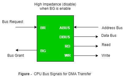
Bus Request : It is used by the DMA controller to request the CPU to relinquish the control of the buses.
Bus Grant : It is activated by the CPU to Inform the external DMA controller that the buses are in high impedance state and the requesting DMA can take control of the buses. Once the DMA has taken the control of the buses it transfers the data. This transfer can take place in many ways.
Types of DMA transfer using DMA controller:
Burst Transfer :
DMA returns the bus after complete data transfer. A register is used as a byte count,
being decremented for each byte transfer, and upon the byte count reaching zero, the DMAC will
release the bus. When the DMAC operates in burst mode, the CPU is halted for the duration of the data
transfer.
Difference between Synchronous and Asynchronous Transmission
Synchronous Transmission:
In Synchronous Transmission, data is sent in form of blocks or frames. This transmission is the full duplex type. Between sender and receiver the synchronization is compulsory. In Synchronous transmission, There is no gap present between data. It is more efficient and more reliable than asynchronous transmission to transfer the large amount of data.
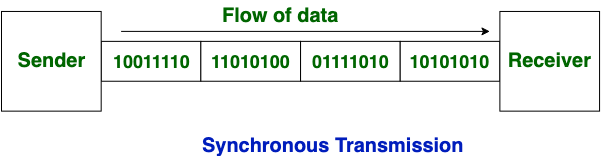
Asynchronous Transmission:
In Asynchronous Transmission, data is sent in form of byte or character. This transmission is the half duplex type transmission. In this transmission start bits and stop bits are added with data. It does not require synchronization.
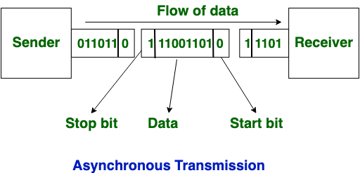
Now, let’s see the difference between Synchronous and Asynchronous Transmission:
S.NOSynchronous TransmissionAsynchronous Transmission
1. In Synchronous transmission, Data is sent in form of blocks or frames. In asynchronous transmission, Data is sent in form of byte or character.
2. Synchronous transmission is fast. Asynchronous transmission is slow.
3. Synchronous transmission is costly. Asynchronous transmission is economical.
4. In Synchronous transmission, time interval of transmission is constant. In asynchronous transmission, time interval of transmission is not constant, it is random.
5. In Synchronous transmission, There is no gap present between data. In asynchronous transmission, There is present gap between data.
6. Efficient use of transmission line is done in synchronous transmission. While in asynchronous transmission, transmission line remains empty during gap in character transmission.
7. Synchronous transmission needs precisely synchronized clocks for the information of new bytes. Asynchronous transmission have no need of synchronized clocks as parity bit is used in this transmission for information of new bytes.
Difference between Multiprocessing and Multiprogramming
1. Multiprocessing :
Multiprocessing is a system that has two or more than one processors. In this, CPUs are added for increasing computing speed of the system. Because of Multiprocessing, there are many processes that are executed simultaneously. Multiprocessing are further classified into two categories: Symmetric Multiprocessing, Asymmetric Multiprocessing.
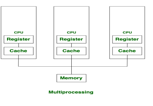
2. Multi-programming :
Multi-programming is more than one process running at a time, it increases CPU utilization by organizing jobs (code and data) so that the CPU always has one to execute. The motive is to keep multiple jobs in main memory. If one job gets occupied with Input/output, CPU can be assigned to other job.
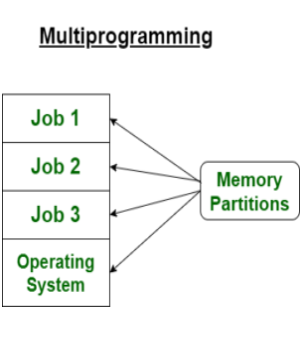
Difference between Multiprocessing and Multiprogramming :
S.No.MultiprocessingMultiprogramming
1. The availability of more than one processor per system, that can execute several set of instructions in parallel is known as multiprocessing. The concurrent application of more than one program in the main memory is known as multiprogramming.
2. The number of CPU is more than one. The number of CPU is one.
3. It takes less time for job processing. It takes more time to process the jobs.
4. In this, more than one process can be executed at a time. In this, one process can be executed at a time.
5. It is economical. It is economical.
6. The number of users is can be one or more than one. The number of users is one at a time.
7. Throughput is maximum. Throughput is less.
8. Its efficiency is maximum. Its efficiency is Less.
Key Differences Between Loosely Coupled and Tightly Coupled Multiprocessor System
The key difference between loosely coupled and tightly coupled system is that loosely coupled system has distributed memory, whereas, the tightly coupled system has shared memory.
Loosely coupled is efficient when the tasks running on different processors has minimal interaction between them. On the other hands, the tightly coupled system can take a higher degree of interaction between processes and is efficient for high-speed and real-time processing.
The loosely coupled system generally do not encounter memory conflict which is mostly experienced by tightly couples system.
The interconnection network in a loosely coupled system is Message Transfer system (MTS) whereas, in a tightly coupled system the interconnection networks are processor-memory interconnection network (PMIN), I/O-processor interconnection network (IOPIN) and the interrupt-signal interconnection network (ISIN).
The data rate of the loosely coupled system is low whereas, the data rate of the tightly coupled system is high.
The loosely coupled system is less expensive but larger in size whereas, the tightly coupled system is more expensive but compact in size.
UNIT 5
Microprogramming
Basis Concepts
Micro-operations: We have already seen that the programs are executed as a sequence of instructions, each instruction consists of a series of steps that make up the instruction cycle fetch, decode, etc. Each of these steps are, in turn, made up of a smaller series of steps called micro-operations.
Micro-operation execution: Each step of the instruction cycle can be decomposed into micro-operation primitives that are performed in a precise time sequence. Each micro-operation is initiated and controlled based on the use of control signals / lines coming from the control unit.
- Controller the data to move from one register to another
- Controller the activate specific ALU functions
Micro-instruction: Each instruction of the processor is translated into a sequence of lower-level micro-instructions. The process of translation and execution are to as microprogramming
Microprogramming: The concept of microprogramming was developed by Maurice Wilkes in 1951, using diode matrices for the memory element. A microprogram consist of a sequence of micro-instructions in a microprogramming.
Microprogrammed Control Unit is a relatively logic circuit that is capable of sequencing through micro-instructions and generating control signal to execute each micro-instruction.
Control Unit: The control Unit is an important portion of the processor.
The control unit issues control signals external to the processor to cause data exchange with memory and I/O unit. The control Unit issues also control signals internal to the processor to move data between registers, to perform the ALU and other internal operations in processor. In a hardwired control unit, the control signals are generated by a micro-instruction are used to controller register transfers and ALU operations. Control Unit design is then the collection and the implementation of all of the needed control signals for the micro-instruction executions.
Hardwired Control Unit –
The control hardware can be viewed as a state machine that changes from one state to another in every clock cycle, depending on the contents of the instruction register, the condition codes and the external inputs. The outputs of the state machine are the control signals. The sequence of the operation carried out by this machine is determined by the wiring of the logic elements and hence named as “hardwired”.
Fixed logic circuits that correspond directly to the Boolean expressions are used to generate the control signals.
Hardwired control is faster than micro-programmed control.
A controller that uses this approach can operate at high speed.
RISC architecture is based on hardwired control unit
Micro-programmed Control Unit –
The control signals associated with operations are stored in special memory units inaccessible by the programmer as Control Words.
Control signals are generated by a program are similar to machine language programs.
Micro-programmed control unit is slower in speed because of the time it takes to fetch microinstructions from the control memory.
Application and advantage of Microprogrammed Control Unit
Micro program :
A program is a set of instructions. An instruction requires a set of micro-operations.
Micro-operations are performed using control signals.
Here, these control signals are generated using micro-instructions.
This means every instruction requires a set of micro-instructions
A set of micro-instructions are called micro-program.
Microprograms for all instructions are stored in a small memory called control memory.
The control memory is present inside the processor.
Working :
Consider an instruction that is fetched from the main memory into the instruction Register (IR). The processor uses its unique opcode to identify the address of the first micro-instruction. That address is loaded into CMAR (Control Memory Address Register). This address is decoded to decide the corresponding memory instruction from the control Memory. Micro-instructions will only have a control field. The control field Indicates the control signals to be generated. Most micro-instructions will not have an address field. Usually µPC will simply get incremented after every micro-instruction.
This is as long as the micro-program is executing sequentially. If there is a branch micro-instruction only then there will be an address filed. If the branch is unconditional, the branch address will be directly loaded into CMAR. For conditional branches, the branch condition will check the appropriate flag. This is done using a MUX which has all flag inputs. If the condition is true, then the mux will inform CMAR to load the branch address. If the condition is false CMAR will simply get incremented.
The control memory is usually implemented using flash ROM as it is non-volatile.
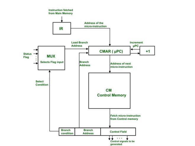
Microprogrammed control unit
Advantages :
The main advantage is flexibility.
Any change in the control unit can be performed by simply changing the micro-instruction.
Can be easily debugged as compared to hardwired control unit.
Most micro-instructions are executed sequentially, they don’t require any address field.
Reduction of size of control memory.
Disadvantages :
Control memory has to be present inside the processor, therefore increases processor size.
This also increases the cost of the processor.
Applications of Microprogrammed Control Unit :
Microprogramming has many advantages like flexibility, simplicity, cost-effectiveness etc.
Therefore, it has a major contribution in the following applications –
Development of control units –
Modern processors have very large and complex instruction sets. Microprogramming is used for making control units of such processors, because it is far less complex and can be easily modified.
High level language support –
Modern high level languages have more advanced and complex data types. Microprogramming can provide support for such data types directly from the processor level. Therefore, the language becomes easy to compile and also faster to execute.
User tailoring of the control unit –
As the control Unit is developed using software, it can be easily reprogrammed. This can be used for custom-made modifications of the Control Unit. For this purpose, the control memory must be writable like RAM or flash ROMs.
Emulation –
Emulation is when one processor (say A) is made to emulate or behave like another processor (say B). To do this, A must be able to execute the instructions of B. If we re-program the control memory of A, same as that of B, then A will be able to emulate the behavior of B, for every instruction. This is possible only in microprogrammed control units.
Used generally when a main processor has to emulate the behavior of a math co-processor.
Improving the operating system –
Microprogramming can be used to implement complex and secure functions of the OS. This not only makes the OS more powerful and efficient, but more importantly secure, as it provides the OS a higher degree of protection from malicious virus attacks.
Micro-Diagnostics or error debugging –
As Microprogrammed Control Units are software based, debugging an error is far more easy as compared to doing the same for a complex hardwired control unit. This allows monitoring, detection and repairs of any kind of system errors in the control unit. It can also use as a runtime substitute, if the corresponding hardwired component fails.
Development of special purpose processors –
All processors are not general purpose. Many applications require special purpose processors like DSP(Digital Signal Processors) for communication, GPU (Graphic Processor Unit) for image processing.
They have complex instruction sets and also need to be constantly upgraded. Microprogrammed control unit is the best choice for them
Machine Instructions
Machine Instructions are commands or programs written in machine code of a machine (computer) that it can recognize and execute.
A machine instruction consists of several bytes in memory that tells the processor to perform one machine operation.
The processor looks at machine instructions in main memory one after another, and performs one machine operation for each machine instruction.
The collection of machine instructions in main memory is called a machine language program.
Machine code or machine language is a set of instructions executed directly by a computer’s central processing unit (CPU). Each instruction performs a very specific task, such as a load, a jump, or an ALU operation on a unit of data in a CPU register or memory. Every program directly executed by a CPU is made up of a series of such instructions.
. Data transfer instructions– move, load exchange, input, output.
MOV :Move byte or word to register or memory .
IN, OUT: Input byte or word from port, output word to port.
LEA: Load effective address
LDS, LES Load pointer using data segment, extra segment .
PUSH, POP: Push word onto stack, pop word off stack.
XCHG: Exchange byte or word.
XLAT: Translate byte using look-up table.
2. Arithmetic instructions – add, subtract, increment, decrement, convert byte/word and compare.
ADD, SUB: Add, subtract byte or word
ADC, SBB :Add, subtract byte or word and carry (borrow).
INC, DEC: Increment, decrement byte or word.
NEG: Negate byte or word (two’s complement).
CMP: Compare byte or word (subtract without storing).
MUL, DIV: Multiply, divide byte or word (unsigned).
IMUL, IDIV: Integer multiply, divide byte or word (signed)
CBW, CWD: Convert byte to word, word to double word
AAA, AAS, AAM,AAD: ASCII adjust for add, sub, mul, div .
DAA, DAS: Decimal adjust for addition, subtraction (BCD numbers)
3. Logic instructions – AND, OR, exclusive OR, shift/rotate and test
NOT : Logical NOT of byte or word (one’s complement)
AND: Logical AND of byte or word
OR: Logical OR of byte or word.
XOR: Logical exclusive-OR of byte or word
TEST: Test byte or word (AND without storing).
SHL, SHR: Logical Shift rotate instruction shift left, right byte or word? by 1or CL
SAL, SAR: Arithmetic shift left, right byte or word? by 1 or CL
ROL, ROR: Rotate left, right byte or word? by 1 or CL .
RCL, RCR: Rotate left, right through carry byte or word? by 1 or CL.
String manipulation instruction – load, store, move, compare and scan for byte/word
MOVS: Move byte or word string
MOVSB, MOVSW: Move byte, word string.
CMPS: Compare byte or word string.
SCAS S: can byte or word string (comparing to A or AX)
LODS, STOS: Load, store byte or word string to AL.
5. Control transfer instructions – conditional, unconditional, call subroutine and return from subroutine.
JMP:Unconditional jump .it includes loop transfer and subroutine and interrupt instructions.
JNZ:jump till the counter value decreases to zero.It runs the loop till the value stored in CX becomes zero
6. Loop control instructions-
LOOP: Loop unconditional, count in CX, short jump to target address.
LOOPE (LOOPZ): Loop if equal (zero), count in CX, short jump to target address.
LOOPNE (LOOPNZ): Loop if not equal (not zero), count in CX, short jump to target address.
JCXZ: Jump if CX equals zero (used to skip code in loop).
Subroutine and Interrupt instructions-
CALL, RET: Call, return from procedure (inside or outside current segment).
INT, INTO: Software interrupt, interrupt if overflow.IRET: Return from interrupt.
What Is an Instruction Set Architecture?
An Instruction Set Architecture (ISA) is part of the abstract model of a computer that defines how the CPU is controlled by the software. The ISA acts as an interface between the hardware and the software, specifying both what the processor is capable of doing as well as how it gets done.
The ISA provides the only way through which a user is able to interact with the hardware. It can be viewed as a programmer’s manual because it’s the portion of the machine that’s visible to the assembly language programmer, the compiler writer, and the application programmer.
The ISA defines the supported data types, the registers, how the hardware manages main memory, key features (such as virtual memory), which instructions a microprocessor can execute, and the input/output model of multiple ISA implementations. The ISA can be extended by adding instructions or other capabilities, or by adding support for larger addresses and data values.
Vector Processing
Vector processing performs the arithmetic operation on the large array of integers or floating-point number. Vector processing operates on all the elements of the array in parallel providing each pass is independent of the other.
We need computers that can solve mathematical problems for us which include, arithmetic operations on the large arrays of integers or floating-point numbers quickly. The general-purpose computer would use loops to operate on an array of integers or floating-point numbers. But, for large array using loop would cause overhead to the processor.
To avoid the overhead of processing loops and fasten the computation, some kind of parallelism must be introduced. Vector processing operates on the entire array in just one operation i.e. it operates on elements of the array in parallel. But, vector processing is possible only if the operations performed in parallel are independent.
Look at the figure below, and compare the vector processing with the general computer processing, you will notice the difference. Below, instructions in both the blocks are set to add two arrays and store the result in the third array. Vector processing adds both the array in parallel by avoiding the use of the loop.
Characteristics of Vector Processing
Each element of the vector operand is a scalar quantity which can either be an integer, floating-point number, logical value or a character. Below we have classified the vector instructions in four types.
Here, V is representing the vector operands and S represents the scalar operands. In the figure below, O1 and O2 are the unary operations and O3 and O4 are the binary operations.
Most of the vector instructions are pipelined as vector instruction performs the same operation on the different data sets repeatedly. Now, the pipelining has start-up delay, so longer vectors would perform better here.
The pipelined vector processors can be classified into two types based on from where the operand is being fetched for vector processing. The two architectural classifications are Memory-to-Memory and Register-to-Register.
In Memory-to-Memory vector processor the operands for instruction, the intermediate result and the final result all these are retrieved from the main memory. TI-ASC, CDC STAR-100, and Cyber-205 use memory-to-memory format for vector instructions.
In Register-to-Register vector processor the source operands for instruction, the intermediate result, and the final result all are retrieved from vector or scalar registers. Cray-1 and Fujitsu VP-200 use register-to-register format for vector instructions.


Comments
Post a Comment