BCA 2ND SEM DIGITAL MCQ
a. 2n-1
b. 2n+1
c. 2n
d. 2n+2
Q2. The boolean functions which can be represented by the sum of minterms and product of maxterms can be categorized in _______.
a. standard form
b. canonical form
c. both a & b
d. none of the above
ANSWER: b. canonical form
Q3. Which illustration from the below stated functions exhibits the conversion of product of maxterm form into sum of minterm form if the value of product of maxterm is F(x,y,z) = π (6,8,10,11) ?
a. F (x,y,z ) = ∑ (7,9,12,13)
b. F (x,y,z) = π (7,9,12,13)
c. F (x,y,z) = σ ( 7,9,12,13)
d. F (x,y,z) = S (7,9,12,13)
ANSWER: a. F (x,y,z ) = ∑ (7,9,12,13)
Q4. Which operation is denoted by the sum-of-product form of boolean expression consisting of AND terms ?
a. ANDing
b. ORing
c. both
d. none of the above
ANSWER: b. ORing
Q5. What are the OR terms present in product of sum form of the boolean expression called as ?
a. minterms
b. maxterms
c. sum terms
d. product terms
ANSWER: c. sum terms
Q6. It is possible to change the non-standard form of boolean function to a standard form by using ______.
a. De-Morgan's Law / Theorem
b. Duality Law / Theorem
c. Complementary Law
d. Distributive Law
ANSWER: d. Distributive Law
Q7. Which combinational circuit is renowned for selecting a single input from multiple inputs & directing the binary information to output line?
a. Data Selector
b. Data Distributer
c. Both a & b
d. None of the above
ANSWER: a. Data Selector
Q8. It is possible for an enable or strobe input to undergo an expansion of two or more mux ICs to the digital multiplexer with the proficiency of large number of _____.
a. inputs
b. outputs
c. selection lines
d. all of the abov
ANSWER: a. inputs
Q9. Which is the major functioning responsibility of the multiplexing combinational circuit?
a. Decoding the binary information
b. Generation of all minterms in an output function with OR-gate
c. Generation of selected path between multiple sources and a single destination
d. All of the above
ANSWER: c. Generation of selected path between multiple sources and a single destination
Q10. Which method of combination circuit implementation is widely adopted with maximum output functions and minimum requirement of ICs?
a. Multiplexer Method
b. Decoder Method
c. Encoder Method
d. Parity Generator Method
ANSWER: b. Decoder Method
Q11. What is the normal operating condition of decoder corresponding to input & output states?
a. E= 0 & Outputs at '0' logic state
b. E = 1 & Outputs at '1' logic state
c. E= 0 & Outputs at '1' logic state
d. E= 1 & Outputs at '0' logic state
ANSWER: a. E= 0 & Outputs at '0' logic state
Q12. Why are the enale lines specifically used for connecting two or more IC packages in accordance to its application in decoder circuit?
a. It allows the reduction of digital function into similar function with more inputs & outputs
b. It allows the expansion of digital function into similar function with more inputs & outputs
c. It allows the reduction of digital function into different function with more inputs & outputs
d. It allows the expansion of digital function into different function with more inputs & outputs
ANSWER: b. It allows the expansion of digital function into similar function with more inputs & outputs
Q13. Which sequential circuits generate the feedback path due to the cross-coupled connection from output of one gate to the input of another gate?
a. Synchronous
b. Asynchronous
c. Both
d. None of the above
ANSWER: b. Asynchronous
Q14. What is/are the crucial function/s of memory elements used in the sequential circuits?
a. Storage of binary information
b. Specify the state of sequential
c. Both a & b
d. None of the above
ANSWER: c. Both a & b
Q15. How are the sequential circuits specified in terms of time sequence?
a. By Inputs
b. By Outputs
c. By Internal states
d. All of the above
ANSWER: d. All of the above
Q16. The behaviour of synchronous sequential circuit can be predicted by defining the signals at ______.
a. discrete instants of time
b. continuous instants of time
c. sampling instants of time
d. at any instant of time
ANSWER: a. discrete instants of time
Q17. Which memory elements are utilized in an asynchronous & clocked sequential circuits respectively?
a. Time- delay devices & registers
b. Time- delay devices & flip-flops
c. Time- delay devices & counters
d. Time-delay devices & latches
ANSWER: b. Time- delay devices & flip-flops
Q18. Why do the D-flipflops receives its designation or nomenclature as 'Data Flipflops' ?
a. Due to its capability to receive data from fliflop
b. Due to its capability to store data in flipflop
c. Due to its capability to transfer the data into flipflop
d. All of the above
ANSWER: c. Due to its capability to transfer the data into flipflop
Q19. The characteristic equation of D-flipflop implies that _____.
a. the next state is dependent on previous state
b. the next state is dependent on present state
c. the next state is independent of previous state
d. the next state is independent of present state
ANSWER: d. the next state is independent of present state
Q20. Which circuit is generated from D-flipflop due to addition of an inverter by causing reduction in the number of inputs?
a. Gated JK- latch
b. Gated SR- latch
c. Gated T- latch
d. Gated D- latch
ANSWER: d. Gated D- latch
Q21. What is the bit storage binary information capacity of any flipflop?
a. 1 bit
b. 2 bits
c. 16 bits
d. infinite bits
ANSWER: a. 1 bit
Q22. What is/are the directional mode/s of shifting the binary information in a shift register?
a. Up-Down
b. Left - Right
c. Front - Back
d. All of the above
View Answer / Hide Answer
ANSWER: b. Left – Right
Q23. Which time interval specify the shifting of overall contents of the shift registers?
a. Bit time
b. Shift time
c. Word time
d. Code time
ANSWER: c. Word time
Q24. A counter is fundamentally a _________ sequential circuit that proceeds through the predetermined sequence of states only when input pulses are applied to it.
a. register
b. memory unit
c. flipflop
d. arithmatic logic unit
ANSWER: a. register
Q25. This set of Computer Fundamentals Multiple Choice Questions & Answers (MCQs) focuses on “SOP & POS”.
1. The terms in SOP are called ___________
a) max terms
b) min terms
c) mid terms
d) sum terms
Explanation: The SOP is the sum of products. It consists of min terms often called the product terms.
Similarly, POS consists of max terms.
Q26. A sum of products expression is a product term (min term) or several min terms ANDed together.
a) True
b) False
Explanation: The statement is partially correct.
A sum of products expression is a product term (min term) or several min terms OR ed(i.e. added) together.
Q27. Which of the following is an incorrect SOP expression?
a) x+x.y
b) (x+y)(x+z)
c) x
d) x+y
Explanation: The second expression is incorrect because it consists of two maxterms ANDed together.
This makes it a POS or the product of sum expression.
Other options are valid SOP expressions.
Q28. The corresponding min term when x=0, y=0 and z=1.
a) x.y.z’
b) X’+Y’+Z
c) X+Y+Z’
d) x’.y’.z
Explanation: The min term is obtained by taking the complement of the zero values and taking the term with value 1 as it is.
Here, x=0,y=0 and z=1, then the min term is x’y’z.
29. LSI stands for ___________
a) Large Scale Integration
b) Large System Integration
c) Large Symbolic Instruction
d) Large Symbolic Integration
Explanation: It stands for large scale integration. This is the abstraction level of the integrated circuits.
It can also be small scale, medium, large or very large scale integration.
30. Which operation is shown in the following expression: (X+Y’).(X+Z).(Z’+Y’)
a) NOR
b) ExOR
c) SOP
d) POS
Explanation: The expression comprises of max terms.
Also, the terms are ANDed together, therefore it is a POS term.
31. The number of min terms for an expression comprising of 3 variables?
a) 8
b) 3
c) 0
d) 1
View Answer
Explanation: If any expression comprises of n variables, its corresponding min terms are given by 2n.
Here, n=3 since there are 3 variables therefore, min terms=23=8.
32. The number of cells in a K-map with n-variables.
a) 2n
b) n2
c) 2n
d) n
View Answer
Explanation: K-map is nothing but Karnaugh map.
SOP and POS expressions can be simplified using the K-map.
The number of cells in case of n-variables=2n.
33. The output of AND gates in the SOP expression is connected using the ________ gate.
a) XOR
b) NOR
c) AND
d) OR
View Answer
Explanation: Since the product terms or the min terms are added in an SOP expression.
Therefore, the OR gate is used to connect the AND gates.
34. The expression A+BC is the reduced form of ______________
a) AB+BC
b) (A+B)(A+C)
c) (A+C)B
d) (A+B)C
View Answer
35.Electronic circuits that operate on one or more input signals to produce standard output _______
a) Series circuits
b) Parallel Circuits
c) Logic Signals
d) Logic Gates
View Answer
Explanation: The logic gates operate on one or more input signals to produce a standard output.
Logic gates give the output in the form of 0 and 1.
The Boolean algebra can be applied to the logic gates.
36. Logic Gates are the building blocks of all circuits in a computer.
a) True
b) False
View Answer
Explanation: The statement is true.
Logic gates are idealized to implement a boolean function in all circuits of a computer.
The signals are directed as per the outputs of the logic gates in the form of 0 and 1.
37. A __________ gate gives the output as 1 only if all the inputs signals are 1.
a) AND
b) OR
c) EXOR
d) NOR
View Answer
Explanation: The AND gate gives a 1 only if all the input signals are 1.
The Boolean expression for evaluating an AND signal is: Y=A.B.
38. The boolean expression of an OR gate is _______
a) A.B
b) A’B+AB’
c) A+B
d) A’B’
View Answer
Explanation: An OR gate gives the result as 1 if any one of the inputs is one.
Its expression is A+B.
An OR gate gives a 0 only if both the inputs are 0.
39. The gate which is used to reverse the output obtained is _____
a) NOR
b) NAND
c) EXOR
d) NOT
View Answer
Explanation: NOT gate is used to reverse the output from 0 to 1 and vice-versa.
The Boolean expression for NOT gate is Y=A’.
Therefore, it gives the complement of the result obtained.
40. Which of the following gate will give a 0 when both of its inputs are 1?
a) AND
b) OR
c) NAND
d) EXOR
View Answer
Explanation: The NAND gate gives 0 as the output when both of its inputs are 1 or any one of the input is 1.
It returns a 1 only if both the inputs are 0.
41. When logic gates are connected to form a gating/logic network it is called as a ______________ logic circuit.
a) combinational
b) sequential
c) systematic
d) hardwired
View Answer
Explanation: It is referred to as a combinational circuit as it comprises a number of gates.
It is connected to evaluate a result of a Boolean expression.
42. The universal gate that can be used to implement any Boolean expression is __________
a) NAND
b) EXOR
c) OR
d) AND
View Answer
Explanation: NAND gate can be used to implement any Boolean expression.
It is a universal gate. A universal gate can be used to implement any other Boolean function without using any other logic gate.
43. The gate which is called an inverter is called _________
a) NOR
b) NAND
c) EXOR
d) NOT
View Answer
Explanation: Inverter is used to reverse the output. A NOT gate is used to invert or change the output from 0 to 1 and vice-versa.
44. The expression of an EXOR gate is ____________
a) A’B+AB’
b) AB+A’B’
c) A+A.B
d) A’+B’
View Answer
Explanation: The expression for an EXOR gate is A’B+AB’.
An EXOR gate is nothing but an exclusive OR gate.
45. A ____________ is a circuit with only one output but can have multiple inputs.
a) Logic gate
b) Truth table
c) Binary circuit
d) Boolean circuit
View Answer
Explanation: A logic gate is used to evaluate a Boolean expression.
It can have multiple inputs but can have only one output.
The different types of logic gates are AND, OR, NOT etc.
46. There are 5 universal gates.
a) True
b) False
View Answer
Explanation: There are only 2 main universal gates: NAND and NOR.
A NAND gate as well as the NOR gate can be used to implement any other Boolean expression thus it is called as a universal gate.
47. The Output is LOW if any one of the inputs is HIGH in case of a _________ gate.
a) NOR
b) NAND
c) OR
d) AND
View Answer
Explanation: In case of NOR Gate the Output is Low (i.e. 0) when any of the Input is High (i.e. 1).
TRUTH TABLE of NOR Gate:-
| A | B | Output |
|---|---|---|
| 0 | 0 | 1 (High) |
| 0 | 1 | 0 (Low) |
| 1 | 0 | 0 (Low) |
| 1 | 1 | 0 (Low) |
This proves it.
48. The following figure shows a ___________ gate.
a) NOR
b) NAND
c) EXOR
d) OR
View Answer
Explanation: The figure is that of a NOR gate.
The bubble signifies that it is a NOR gate.
It is a type of universal gate and can be used to implement all the boolean expressions.
49. The complement of the input given is obtained in case of:
a) NOR
b) AND+NOR
c) NOT
d) EX-OR
View Answer
Explanation: The NOT gate, also called as the inverter gate is used to reverse the input which is given.
It gives an inverted output, thus gives the complement.
Expression for NOT gate: Y=A’, where A is the input.
50. How many AND gates are required to realize the following expression Y=AB+BC?
a) 4
b) 8
c) 1
d) 2
View Answer
Explanation: 2 AND gates are required to realize the expression.
1 AND gate will be used to connect the inputs A and B whereas the other will be used to connect the inputs B and C.
51. Number of outputs in a half adder _____________
a) 1
b) 2
c) 3
d) 0
View Answer
Explanation: A half adder gives two outputs.
One is called the sum and the other is carry.
Half adder can be implemented using an EXOR gate and an AND gate.
52. The ________ gate is an OR gate followed by a NOT gate.
a) NAND
b) EXOR
c) NOR
d) EXNOR
View Answer
Explanation: A NOR gate is a universal gate which is an OR gate followed by a NOT gate.
It therefore reverses the output obtained by an OR gate.
It can be used to implement any Boolean expression.
53. The expression of a NAND gate is_______
a) A.B
b) A’B+AB’
c) (A.B)’
d) (A+B)’
View Answer
Explanation: A NAND gate is an AND gate followed by a NOT gate.
It therefore inverts the output of an AND gate.
NAND gate is also a universal gate.
56. Which of the following correctly describes the distributive law.
a)( A+B)(C+D)=AB+CD
b) (A+B).C=AC+BC
c) (AB)(A+B)=AB
d) (A.B)C=AC.AB
View Answer
11. To display time in railway stations which digital circuit is used?
a) seven segment decoder
b) eight segment encoder
c) 8:3 multiplexer
d) 9 bit segment driver
View Answer
57.Which of the following method is used to minimize Boolean expressions?
- Fourier transform
- Gray code
- Karnaugh mapping
- Venitch method
Answer: Karnaugh mapping
58.Four adjacent ‘1’s in a Karnaugh map forms a
- octet
- singlet
- pair
- quad
Answer: quad
59.If n denotes the number of variable then the number of cells are given as
- 2n
- 2 + n
- 2 – n
- 2n
Answer: 2n
60.A 4-variable Karnaugh map has
- 12 cells
- 16 cells
- 18 cells
- 20 cells
Answer: 16 cells
61.The Boolean expression Y = XY + ZX is in the ___________ form.
- Product-of-Sum
- Sum-of-Products
- Linear
- None of the above
Answer: Sum-of-Products
62.In the Karnaugh map, each cell represents ___________ minterm derived from the Boolean expression.
- 1
- 2
- 3
- 4
Answer: 1
63.Which of the following is NOT considered for forming groups in K-map?
- Rolling
- Diagonal
- Vertical
- Horizontal
Answer: Diagonal
64.The sum or product of two minterms results in
- Maxterms
- Boolean expression
- Implicant
- None of the above
Answer: Implicant
65.While forming groups in K-mapping the Don’t care states are combined along with terms of
- Minterms
- Maxterm
- SOP
- POS
Answer: Minterms
66.Product-of-Sums expressions can be implemented using
- 2-level OR-AND logic circuits
- 2-level NOR logic circuits
- Both
- None
Answer: Both
67.In a Karnaugh map, a group of eight 1’s adjacent to each other is called
- Pairs
- Triad
- Quads
- Octet
Answer: Octet
68.The Boolean expressions are represented in a unique way called
- Canonical form
- Minterm
- Maxterm
- Logic diagram
Answer: Canonical form
69.Don’t care conditions can be used for simplifying Boolean expression in
- Logic diagram
- Minterms
- K-maps
- Maxterms
Answer: K-maps
70.In a Karnaugh map the formation of Quad results in the elimination of _________ variables and their complements.
- 2
- 3
- 4
- 8
Answer: 2
71.A 2-level AND-OR logic circuit is used to express
- Product of sum
- Sum of product
- Boolean expression
- All of the above
Answer: Sum of produt
UNIT 5
1. Memory is a/an ___________
a) Device to collect data from other computer
b) Block of data to keep data separately
c) Indispensable part of computer
d) Device to connect through all over the world
View Answer
Explanation: Memory is an indispensable unit of a computer and microprocessor based systems which stores permanent or temporary data.
2. The instruction used in a program for executing them is stored in the __________
a) CPU
b) Control Unit
c) Memory
d) Microprocessor
View Answer
Explanation: All of the program and the instructions are stored in the memory. The processor fetches it as and when required.
3. A flip flop stores __________
a) 10 bit of information
b) 1 bit of information
c) 2 bit of information
d) 3-bit information
View Answer
Explanation: A flip-flop has capability to store 1 bit of information. It can be used further after erasing previous information.
4. A register is able to hold __________
a) Data
b) Word
c) Nibble
d) Both data and word
View Answer
5. A register file holds __________
a) A large number of word of information
b) A small number of word of information
c) A large number of programs
d) A modest number of words of information
View Answer
Explanation: A register file is different from a simple register because of capability to hold a modest number of words of information. A word is a group of 16-bits or 2-bytes.
6. The very first computer memory consisted of __________
a) A small display
b) A large memory storage equipment
c) An automatic keyboard input
d) An automatic mouse input
View Answer
Explanation: The very first computer memory consisted of a minute magnetic toroid, which required large, bulky circuit boards stored in large cabinates.
7. A minute magnetic toroid is also called as __________
a) Large memory
b) Small memory
c) Core memory
d) Both small and large memory
View Answer
Explanation: A minute magnetic toroid is also called as core memory which is made up of a semiconductor. A semiconductor is a device whose electrical conductivity lies between that of conductor and insulator.
8. Which one of the following has capability to store data in extremely high densities?
a) Register
b) Capacitor
c) Semiconductor
d) Flip-Flop
View Answer
Explanation: Semiconductor has capability to store data in extremely high densities.
9. A large memory is compressed into a small one by using __________
a) LSI semiconductor
b) VLSI semiconductor
c) CDR semiconductor
d) SSI semiconductor
View Answer
Explanation: VLSI (Very Large Scale Integration) semiconductor is used in modern computers to short the size of memory.
10. VLSI chip utilizes __________
a) NMOS
b) CMOS
c) BJT
d) All of the Mentioned
View Answer
Explanation: VLSI (Very Large Scale Integration) is a memory chip which is made up of NMOS, CMOS, BJT, and BiCMOS. It can include 10,000 to 100,000 gates per IC.
11. CD-ROM refers to __________
a) Floppy disk
b) Compact Disk-Read Only Memory
c) Compressed Disk-Read Only Memory
d) Compressed Disk- Random Access Memory
View Answer
Explanation: CD-ROM refers to Compact Disk-Read Only Memory.
12. Data stored in an electronic memory cell can be accessed at random and on demand using __________
a) Memory addressing
b) Direct addressing
c) Indirect addressing
d) Control Unit
View Answer
Explanation: Direct addressing eliminates the need to process a large stream of irrelevant data in order to the desired data word.
13. The full form of PLD is __________
a) Programmable Large Device
b) Programmable Long Device
c) Programmable Logic Device
d) Programmable Lengthy Device
View Answer
Explanation: The full form of PLD is Programmable Logic Device.
14. The evolution of PLD began with __________
a) EROM
b) RAM
c) PROM
d) EEPROM
View Answer
Explanation: The evolution of PLD (Programmable Logic Device) began with Programmable Read Only Memory (i.e. PROM). Here, the ROM can be externally programmed as per the user.
15. A ROM is defined as __________
a) Read Out Memory
b) Read Once Memory
c) Read Only Memory
d) Read One Memory
View Answer
Explanation: A ROM is defined as Read Only Memory which can read the instruction stored in a computer.
1. The full form of ROM is __________
a) Read Outside Memory
b) Read Out Memory
c) Read Only Memory
d) Read One Memory
View Answer
Explanation: The full form of ROM is Read Only Memory.
2. ROM consist of __________
a) NOR and OR arrays
b) NAND and NOR arrays
c) NAND and OR arrays
d) NOR and AND arrays
View Answer
Explanation: ROM consists of NAND and OR arrays which can be programmed by the user to implement combinational & sequential functions. Combinational Operations like that of adders and subtractors and Sequential Functions like that of storing in the memory.
3. For reprogrammability, PLDs use __________
a) PROM
b) EPROM
c) CDROM
d) PLA
View Answer
Explanation: For reprogrammability, PLDs use EPROM (i.e. Erasable PROM). It erases the previous program and starts uploading a new one. However, data is erased by exposing it to UV-light, which is a tedious and time-consuming process.
4. The full form of PROM is __________
a) Previous Read Only Memory
b) Programmable Read Out Memory
c) Programmable Read Only Memory
d) Previous Read Out Memory
View Answer
Explanation: The full form of PROM is Programmable Read Only Memory, where the ROM can be programmed by the user.
5. The full form of EPROM is __________
a) Easy Programmable Read Only Memory
b) Erasable Programmable Read Only Memory
c) Eradicate Programmable Read Only Memory
d) Easy Programmable Read Out Memory
View Answer
Explanation: The full form of EPROM is Erasable Programmable Read Only Memory, where the ROM can be erased and re-used by the user.
6. PLDs with programmable AND and fixed OR arrays are called __________
a) PAL
b) PLA
c) APL
d) PPL
View Answer
Explanation: PLDs with programmable AND and fixed OR arrays are called PAL (i.e. Programmable Array Logic). However, PAL is less flexible but has higher speed.
7. When both the AND and OR are programmable, such PLDs are known as __________
a) PAL
b) PPL
c) PLA
d) APL
View Answer
Explanation: When both the AND and OR are programmable, such PLDs are known as PLA (i.e. Programmable Logic Array). However, PLA is more flexible but has less speed.
8. ASIC stands for __________
a) Application Special Integrated Circuits
b) Applied Special Integrated Circuits
c) Application Specific Integrated Circuits
d) Applied Specific Integrated Circuits
View Answer
Explanation: In digital electronics, ASIC stands for Application Specific Integrated Circuits. It is a customized integrated circuit which is produced for a specific use and not for a common-purpose.
9. The programmability and high density of PLDs make them useful in the design of __________
a) ISAC
b) ASIC
c) SACC
d) CISF
View Answer
Explanation: The programmability and high density of PLDs make them useful in the design of ASIC (i.e. Application Specific Integrated Circuits) where design changes can be more rapidly and inexpensively.
10. FPGA stands for __________
a) Full Programmable Gate Array
b) Full Programmable Genuine Array
c) First Programmable Gate Array
d) Field Programmable Gate Array
View Answer
Explanation: In digital electronics, FPGA stands for Field Programmable Gate Array. This type of integrated circuit is for general-purpose which is configured by the user as per their requirement.
11. Which of the following is a reprogrammable gate array?
a) EPROM
b) FPGA
c) Both EPROM and FPGA
d) ROM
View Answer
Explanation: Both FPGA and EPROM are reprogrammable gate array.
12. The difference between FPGA and PLD is that __________
a) FPGA is slower than PLD
b) FPGA has high power dissipation
c) FPGA incorporates logic blocks
d) All of the Mentioned
View Answer
Explanation: The difference between FPGA and PLD is that FPGA incorporates logic blocks instead of fixed AND-OR gates and is faster with low power dissipation. FPGAs are designed for having higher gate count whereas, PLDs are used for lesser gate counts.
1. Memories are classified into _____ categories.
a) 3
b) 4
c) 5
d) 6
View Answer
Explanation: Memory is typically classified of 2 types: Primary and Secondary. These are further classified into 5 types of memories and these are Secondary, RAM, Dynamic/Static, Volatile/Non-volatile, Magnetic/Semiconductor Memory.
2. Secondary memory is also known as ___________
a) Registers
b) Main Memory
c) RAM
d) Both registers and main memory
View Answer
Explanation: Secondary memory is also known as Registers/Main Memory. In secondary memory, data is usually stored for a long-term.
3. In a computer, registers are present __________
a) Within control unit
b) Within RAM
c) Within ROM
d) Within CPU
View Answer
Explanation: In a computer, registers are present within the CPU to store data temporarily during arithmetic and logical operations and during the functioning of the ALU.
4. Which of the following has the lowest access time?
a) RAM
b) ROM
c) Registers
d) Flag
View Answer
Explanation: Registers has the lowest access time, as they are available inside the CPU. Registers are present within the CPU to store data temporarily during arithmetic and logical operations and during the functioning of the ALU.
5. Main memories of a computer, usually made up of __________
a) Registers
b) Semiconductors
c) Counters
d) PLDs
View Answer
Explanation: Main memories of a computer, usually made up of semiconductors which are available external to the CPU to store program and data during execution of a program. Registers are present within the CPU to store data temporarily during arithmetic and logical operations and during the functioning of the ALU.
6. As the storage capacity of the main memory is inadequate, which memory is used to enhance it?
a) Secondary Memory
b) Auxiliary Memory
c) Static Memory
d) Both Secondary Memory and Auxiliary Memory
View Answer
Explanation: As the storage capacity of the main memory is inadequate, Secondary memory is used to enhance it and it is also known as auxiliary memory. Secondary memory is also known as Registers/Main Memory. In secondary memory, data is usually stored for a long-term.
7. Which memories are if magnetic memory type?
a) Main Memory
b) Secondary Memory
c) Static Memory
d) Volatile Memory
View Answer
Explanation: Usually, secondary memories are of magnetic memory type that are used to store large type quantities of data. In secondary memory, data is usually stored for a long-term.
8. Which of the following comes under secondary memory/ies?
a) Floppy disk
b) Magnetic drum
c) Hard disk
d) All of the Mentioned
View Answer
Explanation: All of the mentioned equipments are of external storage which is known as secondary memories. In secondary memory, data is usually stored for a long-term.
9. Based on method of access, memory devices are classified into ____________ categories.
a) 2
b) 3
c) 4
d) 5
View Answer
Explanation: Based on the method of access, memory devices are classified into two categories and these are sequential access memory and RAM. A sequential access memory is one in which a particular memory location is accessed sequentially.
10. A sequential access memory is one in which __________
a) A particular memory location is accessed rapidly
b) A particular memory location is accessed sequentially
c) A particular memory location is accessed serially
d) A particular memory location is accessed parallely
View Answer
Explanation: A sequential access memory is one in which A particular memory location is accessed sequentially (i.e. the ith memory location is accessed only after sequencing through previous (i-1) memory locations).
11. An example of sequential access memory is __________
a) Floppy disk
b) Hard disk
c) Magnetic tape memory
d) RAM
View Answer
Explanation: A sequential access memory is one in which a particular memory location is accessed sequentially. In magnetic tape memory, data is accessed sequentially.
12. A Random Access Memory is one in which __________
a) Any location can be accessed sequentially
b) Any location can be accessed randomly
c) Any location can be accessed serially
d) Any location can be accessed parallely
View Answer
Explanation: A Random Access Memory is one in which any location can be accessed randomly.
13. An example of RAM is __________
a) Floppy disk
b) Hard disk
c) Magnetic tape memory
d) Semiconductor RAM
View Answer
Explanation: A Random Access Memory is one in which any location can be accessed randomly. A semiconductor RAM is too much fast and can occupy any space in the memory location.
14. A static memory is one in which __________
a) Content changes with time
b) Content doesn’t changes with time
c) Memory is static always
d) Memory is dynamic always
View Answer
Explanation: A static memory is one in which content doesn’t changes with time (i.e. stable). Dynamic memory is one in which content changes with time (i.e. unstable).
15. A dynamic memory is one in which __________
a) Content changes with time
b) Content doesn’t changes with time
c) Memory is static always
d) Memory is dynamic always
View Answer
Explanation: A static memory is one in which content doesn’t change with time (i.e. stable). Dynamic memory is one in which content changes with time (i.e. unstable).
. Dynamic memory cells use _______________ as the storage device.
a) The reactance of a transistor
b) The impedance of a transistor
c) The capacitance of a transistor
d) The inductance of a transistor
View Answer
Explanation: Capacitance of a transistor prevents from loss of information in a dynamic memory cell.
2. To store 1-bit of information, how many transistor is/are used ____________
a) 1
b) 2
c) 3
d) 4
View Answer
Explanation: Only one bit transistor is needed to store 1-bit of information.
3. Static memory holds data as long as __________
a) AC power is applied
b) DC power is applied
c) Capacitor is fully charged
d) High Conductivity
View Answer
Explanation: In any semiconductor equipment, AC power can’t be supplied directly. So, static memory holds the data as long as DC power is applied.
4. The example of dynamic memory is __________
a) CCD
b) Semiconductor dynamic RAM
c) Both CCD and semiconductor dynamic RAM
d) Floppy-Disk
View Answer
Explanation: The examples of dynamic memories are CCD and semiconductor dynamic RAM because of the contents of both the memories changes with time.
5. In dynamic memory, CCD stands for __________
a) Charged Count Devices
b) Change Coupled Devices
c) Charge Coupled Devices
d) Charged Compact Disk
View Answer
Explanation: In dynamic memory, CCD stands for Charge Coupled Devices.
6. Volatile memory refers to __________
a) The memory whose loosed data is achieved again when power to the memory circuit is removed
b) The memory which looses data when power to the memory circuit is removed
c) The memory which looses data when power to the memory circuit is applied
d) The memory whose loosed data is achieved again when power to the memory circuit is applied
View Answer
Explanation: Volatile means ‘liable to change rapidly’ and volatile memory refers to the memory which looses data rapidly when power to the memory circuit is removed. Thus, it looks after it’s data as long as it is powered. Non-volatile means ‘not volatile’ and non-volatile memory refers to the memory which retains the data even if there is a break in the power supply.
7. Non-volatile memory refers to __________
a) The memory whose loosed data is retained again when power to the memory circuit is removed/applied
b) The memory which looses data when power to the memory circuit is removed
c) The memory which looses data when power to the memory circuit is applied
d) The memory whose loosed data is achieved again when power to the memory circuit is applied
View Answer
Explanation: Volatile means ‘liable to change rapidly’ and volatile memory refers to the memory which looses data rapidly when power to the memory circuit is removed. Thus, it looks after it’s data as long as it is powered. Non-volatile means ‘not volatile’ and non-volatile memory refers to the memory which retains the data even if there is a break in the power supply.
8. The example of non-volatile memory device is __________
a) Magnetic Core Memory
b) Read Only Memory
c) Random Access Memory
d) Both Magnetic Core Memory and Read Only Memory
View Answer
Explanation: Non-volatile means ‘not volatile’ and non-volatile memory refers to the memory which retains the data even if there is a break in the power supply. The examples of non-volatile memory devices are Magnetic Core Memory & ROM because both have capability to retain the data.
9. Based on material used for construction, memory devices are classifieds into ________ categories.
a) 2
b) 3
c) 4
d) 5
View Answer
Explanation: Based on material used for construction, memory devices are classifieds into two categories, viz., Magnetic and Semiconductor memory. Magnetic recording is the process of storing data magnetically. Hard disk, floppy disk, magnetic tape are examples of magnetic recording process.
10. Magnetic recording is the process of __________
a) Storing data symmetrically
b) Storing data sequentially
c) Storing data magnetically
d) Both storing data symmetrically and
View Answer
Explanation: Based on material used for construction, memory devices are classifieds into two categories, viz., Magnetic and Semiconductor memory. Magnetic recording is the process of storing data magnetically. Hard disk, floppy disk, magnetic tape are examples of the magnetic recording process.
11. Magnetic drum is a storage medium using __________
a) The surface of a jumping magnetic drum
b) The surface of a rotating magnetic drum
c) The surface of a stopped magnetic drum
d) The surface of a moving magnetic drum
View Answer
Explanation: Magnetic drum is a storage medium using the surface of a rotating magnetic drum which have tendency to hold the data.
12. Magnetic core is the digital memory in which data is stored magnetically in individual cores operated by __________
a) Up and down select wires
b) Row and column select wires
c) Serial and parallel select wires
d) Up and Serial select wires
View Answer
Explanation: Magnetic core is the digital memory in which data is stored magnetically in individual cores operated by row and column select wires, with data obtained from sense wire.
13. By which technology, semiconductor memories are constructed?
a) PLD
b) LSI
c) VLSI
d) Both LSI and VLSI
View Answer
Explanation: Generally, semiconductor memories are constructed using Large Scale Integration (LSI) or Very Large Scale Integration (VLSI) because these are made up of NMOS, CMOS, BJT, etc.
1. When two or more devices try to write data in a bus simultaneously, is known as ______________
a) Bus collisions
b) Address multiplexing
c) Address decoding
d) Bus contention
View Answer
Explanation: Bus contention is an undesirable state of the bus of a computer, in which more than one memory mapped device or the CPU is attempting to place output values onto the bus at once.
2. A memory is a collection of ____________
a) Unit cells
b) Storage cells
c) Data cells
d) Binary cells
View Answer
Explanation: A memory is a collection of storage cells with associated circuits needed to transfer information.
3. To transfer the information from input to output and vice versa, the cells used are ____________
a) Storage cells
b) Data cells
c) Unit cells
d) Both data and unit cells
View Answer
Explanation: To transfer the information from input to output and vice versa, the cells used are called storage cells. The storage cells stores data in the form of binary information.
4. The data stored in a group of bits is called ____________
a) Nibble
b) Word
c) Byte
d) Address
View Answer
Explanation: The data stored in a group of bits is called word. Usually, a word is a group of 16-bits or 2-bytes.
5. Each word consist of a sequence of ____________
a) Letters
b) Binary numbers
c) Hexadecimal numbers
d) Gray codes
View Answer
Explanation: Each word consists of a sequence of 0s and 1s (i.e. binary numbers). Usually, a word is a group of 16-bits or 2-bytes.
6. Each word stored in a memory location is represented by ____________
a) RAM
b) ROM
c) Storage class
d) Address
View Answer
Explanation: Each word stored in a memory location is represented by address. Usually, a word is a group of 16-bits or 2-bytes.
7. The group of each 8-bit is called ____________
a) Nibble
b) Flag
c) Byte
d) Word
View Answer
Explanation: 1 byte = 8-bit, 4-bits = 1 nibble and 16-bits = 1 word.
8. The capacity of a memory unit is ____________
a) The number of binary input stored
b) The number of words stored
c) The number of bytes stored
d) All of the Mentioned
View Answer
Explanation: The total number of bytes that can be stored, is the maximum capacity of a memory unit. However, memory unit is the smallest unit of a processor.
9. The communication between memory and its environment is achieved through ____________
a) Control lines
b) Data input/output lines
c) Address selection lines
d) All of the Mentioned
View Answer
Explanation: Firstly, the data input is needed to transfer the information and it is passed through the address lines and then controlled by control lines. The control lines are responsible for the timing and control of the signals sent and received.
10. One of the most important specifications on magnetic media is the ____________
a) Polarity reversal rate
b) Tracks per inch
c) Data transfer rate
d) Rotation speed
View Answer
Explanation: The rate of data transfer depends on the properties of magnetic media.
1. Which of the following has the capability to store the information permanently?
a) RAM
b) ROM
c) Storage cells
d) Both RAM and ROM
View Answer
Explanation: ROM (Read Only Memory) has the capability to store the information permanently. RAM provides random access to memory. Storage cells are responsible for the transfer of data from and into the memory.
2. ROM has the capability to perform _____________
a) Write operation only
b) Read operation only
c) Both write and read operation
d) Erase operation
View Answer
Explanation: ROM means “Read Only Memory”. Hence, it has the capability to perform read operation only. No write or erase operation could be performed in the ROM.
3. Since, ROM has the capability to read the information only then also it has been designed, why?
a) For controlling purpose
b) For loading purpose
c) For booting purpose
d) For erasing purpose
View Answer
Explanation: ROM means “Read Only Memory”. Hence, it has capability to perform read operation only. No write or erase operation could be performed in the ROM. It has designed to provide the computer with resident programmes and for booting purpose.
4. The ROM is a ___________
a) Sequential circuit
b) Combinational circuit
c) Magnetic circuit
d) Static circuit
View Answer
Explanation: ROM is a combination of different ICs. So, it is a combinational circuit. It depends on present input and not past states.
5. ROM is made up of ___________
a) NAND and OR gates
b) NOR and decoder
c) Decoder and OR gates
d) NAND and decoder
View Answer
Explanation: ROM (Read Only Memory) has the capability to store the information permanently. ROM is made up of decoder and OR gates within a single IC package.
6. Why are ROMs called non-volatile memory?
a) They lose memory when power is removed
b) They do not lose memory when power is removed
c) They lose memory when power is supplied
d) They do not lose memory when power is supplied
View Answer
Explanation: Volatile memory stores data as long as it is powered. ROMs are called non-volatile memory because of they do not lose memory when power is removed.
7. In ROM, each bit is a combination of the address variables is called ___________
a) Memory unit
b) Storage class
c) Data word
d) Address
View Answer
Explanation: In ROM, each bit combination that comes out of the output lines is called data word. Usually, a word consists of 16-bits or 2-bytes.
8. Which is not a removable drive?
a) Zip
b) Hard disk
c) Super Disk
d) Jaz
View Answer
Explanation: Hard disk is present inside a computer. So, it is not a removable drive.
9. In ROM, each bit combination that comes out of the output lines is called ___________
a) Memory unit
b) Storage class
c) Data word
d) Address
View Answer
Explanation: In ROM, each bit combination that comes out of the output lines is called data word. Usually, a word consists of 16-bits or 2-bytes.
10. VLSI chip utilizes ___________
a) NMOS
b) CMOS
c) BJT
d) All of the Mentioned
View Answer
Explanation: Very Large Scale Integration (VLSI) (ranging from 10,000 to 100,000 gates per IC) is a memory chip which is made up of NMOS, CMOS, BJT, and BiCMOS.
1. In parts of the
processor, adders are used to calculate ____________
a) Addresses
b) Table indices
c) Increment and decrement operators
d) All of the Mentioned
View
Answer
Answer: d
Explanation: Adders are used to perform the operation of addition. Thus, in
parts of the processor, adders are used to calculate addresses, table indices,
increment and decrement operators, and similar operations.
2. Total number of
inputs in a half adder is __________
a) 2
b) 3
c) 4
d) 1
View
Answer
Answer: a
Explanation: Total number of inputs in a half adder is two. Since an EXOR gates
has 2 inputs and carry is connected with the input of EXOR gates. The output of
half-adder is also 2, them being, SUM and CARRY. The output of EXOR gives SUM
and that of AND gives carry.
3. In which operation
carry is obtained?
a) Subtraction
b) Addition
c) Multiplication
d) Both addition and subtraction
View
Answer
Answer: b
Explanation: In addition, carry is obtained. For example: 1 0 1 + 1 1 1 = 1 0
0; in this example carry is obtained after 1st addition (i.e. 1 + 1 = 1 0). In
subtraction, borrow is obtained. Like, 0 – 1 = 1 (borrow 1).
Subscribe Now: Digital Electronics Newsletter | Important Subjects Newsletters
advertisement
4. If A and B are the
inputs of a half adder, the sum is given by __________
a) A AND B
b) A OR B
c) A XOR B
d) A EX-NOR B
View
Answer
Answer: c
Explanation: If A and B are the inputs of a half adder, the sum is given by A
XOR B, while the carry is given by A AND B.
5. If A and B are the
inputs of a half adder, the carry is given by __________
a) A AND B
b) A OR B
c) A XOR B
d) A EX-NOR B
View
Answer
Answer: a
Explanation: If A and B are the inputs of a half adder, the carry is given by:
A(AND)B, while the sum is given by A XOR B.
Become Top Ranker in Digital Circuits Now!
6. Half-adders have a
major limitation in that they cannot __________
a) Accept a carry bit from a present stage
b) Accept a carry bit from a next stage
c) Accept a carry bit from a previous stage
d) Accept a carry bit from the following stages
View
Answer
Answer: c
Explanation: Half-adders have a major limitation in that they cannot accept a
carry bit from a previous stage, meaning that they cannot be chained together
to add multi-bit numbers. However, the two output bits of a half-adder can also
represent the result A+B=3 as sum and carry both being high.
7. The difference between
half adder and full adder is __________
a) Half adder has two inputs while full adder has four inputs
b) Half adder has one output while full adder has two outputs
c) Half adder has two inputs while full adder has three inputs
d) All of the Mentioned
View
Answer
Answer: c
Explanation: Half adder has two inputs while full adder has three outputs; this
is the difference between them, while both have two outputs SUM and CARRY.
8. If A, B and C are
the inputs of a full adder then the sum is given by __________
a) A AND B AND C
b) A OR B AND C
c) A XOR B XOR C
d) A OR B OR C
View
Answer
Answer: c
Explanation: If A, B and C are the inputs of a full adder then the sum is given
by A XOR B XOR C.
9. If A, B and C are
the inputs of a full adder then the carry is given by __________
a) A AND B OR (A OR B) AND C
b) A OR B OR (A AND B) C
c) (A AND B) OR (A AND B)C
d) A XOR B XOR (A XOR B) AND C
View
Answer
Answer: a
Explanation: If A, B and C are the inputs of a full adder then the carry is
given by A AND B OR (A OR B) AND C, which is equivalent to (A AND B) OR (B AND
C) OR (C AND A).
10. How many AND, OR
and EXOR gates are required for the configuration of full adder?
a) 1, 2, 2
b) 2, 1, 2
c) 3, 1, 2
d) 4, 0, 1
View
Answer
Answer: b
1. Half subtractor is
used to perform subtraction of ___________
a) 2 bits
b) 3 bits
c) 4 bits
d) 5 bits
View
Answer
Answer: a
Explanation: Half subtractor is a combinational circuit which is used to
perform subtraction of two bits, namely minuend and subtrahend and produces two
outputs, borrow and difference.
2. For subtracting 1
from 0, we use to take a _______ from neighbouring bits.
a) Carry
b) Borrow
c) Input
d) Output
View
Answer
Answer: b
Explanation: For subtracting 1 from 0, we use to take a borrow from
neighbouring bits because carry is taken into consideration during addition
process.
3. How many outputs
are required for the implementation of a subtractor?
a) 1
b) 2
c) 3
d) 4
View
Answer
Answer: b
Explanation: There are two outputs required for the implementation of a
subtractor. One for the difference and another for borrow.
Note: Join free Sanfoundry classes at Telegram or Youtube
advertisement
4. Let the input of a
subtractor is A and B then what the output will be if A = B?
a) 0
b) 1
c) A
d) B
View
Answer
Answer: a
Explanation: The output for A = B will be 0. If A = B, it means that A = B = 0
or A = B = 1. In both of the situation subtractor gives 0 as the output.
5. Let A and B is the
input of a subtractor then the output will be ___________
a) A XOR B
b) A AND B
c) A OR B
d) A EXNOR B
View
Answer
Answer: a
Explanation: The subtractor has two outputs BORROW and DIFFERENCE. Since the
difference output of a subtractor is given by AB’ + BA’ and this is the output
of a XOR gate. So, the final difference output is AB’ + BA’.
Take Digital Circuits Mock Tests -
Chapterwise!
Start the Test Now: Chapter 1, 2, 3, 4, 5, 6, 7, 8, 9, 10
6. Let A and B is the
input of a subtractor then the borrow will be ___________
a) A AND B’
b) A’ AND B
c) A OR B
d) A AND B
View
Answer
Answer: b
Explanation: The borrow of a subtractor is received through AND gate whose one
input is inverted. On that basis the borrow will be (A’ AND B).
7. What does minuend
and subtrahend denotes in a subtractor?
a) Their corresponding bits of input
b) Its outputs
c) Its inputs
d) Borrow bits
View
Answer
Answer: c
Explanation: Minuend and subtrahend are the two bits of input of a subtractor.
If A and B are the two inputs of a subtractor then A is called minuend and B as
subtrahend.
8. Full subtractor is
used to perform subtraction of ___________
a) 2 bits
b) 3 bits
c) 4 bits
d) 8 bits
View
Answer
Answer: b
Explanation: Full subtractor is used to perform subtraction of 3 bits, namely
minuend bit, subtrahend bit and borrow from the previous stage. However, it
also produces 2 outputs BORROW and DIFFERENCE.
9. The full subtractor
can be implemented using ___________
a) Two XOR and an OR gates
b) Two half subtractors and an OR gate
c) Two multiplexers and an AND gate
d) Two comparators and an AND gate
View
Answer
Answer: b
Explanation: A full subtractor has 3 input bits and two outputs bits BORROW and
DIFFERENCE. The full subtractor can be implemented using two half subtractors
and an OR gate.
10. The output of a
subtractor is given by (if A, B and X are the inputs).
a) A AND B XOR X
b) A XOR B XOR X
c) A OR B NOR X
d) A NOR B XOR X
View
Answer
Answer: b
Explanation: The difference output of a subtractor is given by (if A, B and X
are the inputs) A XOR B XOR X.
11. The output of a
full subtractor is same as ____________
a) Half adder
b) Full adder
c) Half subtractor
d) Decoder
View
Answer
Answer: b
Explanation: The sum and difference output of a full adder and a full
subtractor are same. If A, B and C are the input of a full adder and a full
subtractor then the output will be given by (A XOR B XOR C), respectively.
1. What is a
multiplexer?
a) It is a type of decoder which decodes several inputs and gives one output
b) A multiplexer is a device which converts many signals into one
c) It takes one input and results into many output
d) It is a type of encoder which decodes several inputs and gives one output
View
Answer
Answer: b
Explanation: A multiplexer (or MUX) is a device that selects one of several
analog or digital input signals and forwards the selected input into a single
line, depending on the active select lines.
2. Which combinational
circuit is renowned for selecting a single input from multiple inputs & directing
the binary information to output line?
a) Data Selector
b) Data distributor
c) Both data selector and data distributor
d) DeMultiplexer
View
Answer
Answer: a
Explanation: Data Selector is another name of Multiplexer. A multiplexer (or
MUX) is a device that selects one of several analog or digital input signals
and forwards the selected input into a single line, depending on the active
select lines.
3. It is possible for
an enable or strobe input to undergo an expansion of two or more MUX ICs to the
digital multiplexer with the proficiency of large number of ___________
a) Inputs
b) Outputs
c) Selection lines
d) Enable lines
View
Answer
Answer: a
Explanation: It is possible for an enable or strobe input to undergo an
expansion of two or more MUX ICs to the digital multiplexer with the
proficiency of large number of inputs.
Sanfoundry Certification Contest of the Month is Live. 100+ Subjects. Participate Now!
advertisement
4. Which is the major functioning
responsibility of the multiplexing combinational circuit?
a) Decoding the binary information
b) Generation of all minterms in an output function with OR-gate
c) Generation of selected path between multiple sources and a single
destination
d) Encoding of binary information
View
Answer
Answer: c
Explanation: The major functioning responsibility of the multiplexing
combinational circuit is generation of selected path between multiple sources
and a single destination because it makes the circuit too flexible. A
multiplexer (or MUX) is a device that selects one of several analog or digital
input signals and forwards the selected input into a single line, depending on
the active select lines.
5. What is the
function of an enable input on a multiplexer chip?
a) To apply Vcc
b) To connect ground
c) To active the entire chip
d) To active one half of the chip
View
Answer
Answer: c
Explanation: Enable input is used to active the chip, when enable is high the
chip works (ACTIVE), when enable is low the chip does not work (MEMORY).
However, Enable can be Active-High or Active-Low, indicating it is active
either when it is connected to VCC or GND respectively.
Check this: Electronics & Communication Engineering Books | Electrical Engineering MCQs
6. One multiplexer can
take the place of ___________
a) Several SSI logic gates
b) Combinational logic circuits
c) Several Ex-NOR gates
d) Several SSI logic gates or combinational logic circuits
View
Answer
Answer: d
Explanation: A multiplexer (or MUX) is a device that selects one of several
analog or digital input signals and forwards the selected input into a single
line, depending on the active select lines. Since many operational behaviour
can be performed by using a multiplexer. Whereas, a combinational circuit is a
combination of many logic gates which makes the circuit more complex.
7. A digital
multiplexer is a combinational circuit that selects ___________
a) One digital information from several sources and transmits the selected one
b) Many digital information and convert them into one
c) Many decimal inputs and transmits the selected information
d) Many decimal outputs and accepts the selected information
View
Answer
Answer: a
Explanation: A digital multiplexer is a combinational circuit that selects one
digital information from several sources and transmits the selected information
on a single output line depending on the status of the select lines. That is
why it is also known as a data selector.
8. In a multiplexer,
the selection of a particular input line is controlled by ___________
a) Data controller
b) Selected lines
c) Logic gates
d) Both data controller and selected lines
View
Answer
Answer: b
Explanation: The selection of a particular input line is controlled by a set of
selected lines in a multiplexer, which helps to select a particular input from
several sources.
9. If the number of n
selected input lines is equal to 2^m then it requires _____ select lines.
a) 2
b) m
c) n
d) 2n
View
Answer
Answer: b
Explanation: If the number of n selected input lines is equal to 2^m then it
requires m select lines to select one of m select lines.
10. How many select
lines would be required for an 8-line-to-1-line multiplexer?
a) 2
b) 4
c) 8
d) 3
View
Answer
Answer: d
Explanation: 2n input lines, n control lines and 1
output line available for MUX. Here, 8 input lines mean 23 inputs. So, 3 control lines are possible. Depending on the
status of the select lines, the input is selected and fed to the output.
11. A basic
multiplexer principle can be demonstrated through the use of a ___________
a) Single-pole relay
b) DPDT switch
c) Rotary switch
d) Linear stepper
View
Answer
Answer: c
Explanation: A basic multiplexer principle can be demonstrated through the use
of a rotary switch. Since its behaviour is similar to the multiplexer. There
are around 10 digits out of which one is selected one at a time and fed to the
output.
12. How many NOT gates
are required for the construction of a 4-to-1 multiplexer?
a) 3
b) 4
c) 2
d) 5
View
Answer
Answer: c
Explanation: There are two NOT gates required for the construction of 4-to-1
multiplexer. x0, x1, x2 and x3 are the inputs and C1 and C0 are the select
lines and M is the output.
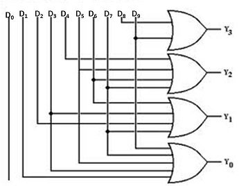
The diagram of a 4-to-1 multiplexer is shown below: 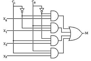
13. In the given
4-to-1 multiplexer, if c1 = 0 and c0 = 1 then the output M is ___________
a) X0
b) X1
c) X2
d) X3
View
Answer
Answer: b
Explanation: The output will be X1, because c1 = 0 and c0 = 1 results into 1
which further results as X1. And rest of the AND gates gives output as 0.
14. The enable input
is also known as ___________
a) Select input
b) Decoded input
c) Strobe
d) Sink
View
Answer
Answer: c
1. 4 to 1 MUX would
have ____________
a) 2 inputs
b) 3 inputs
c) 4 inputs
d) 5 inputs
View
Answer
Answer: c
Explanation: 4 to 1 multiplexer would have 4 inputs (X0, X1, X2, X3), 2 select
lines (C1, C0) and 1 output (M). It can be observed from this diagram:

2. The two input MUX
would have ____________
a) 1 select line
b) 2 select lines
c) 4 select lines
d) 3 select lines
View
Answer
Answer: a
Explanation: The two input multiplexer would have n select lines in 2n. Thus n =1. Therefore, it has 1 select line.
3. A combinational
circuit that selects one from many inputs are ____________
a) Encoder
b) Decoder
c) Demultiplexer
d) Multiplexer
View
Answer
Answer: d
Explanation: A combinational circuit that selects one from many inputs is known
as Multiplexer. Whereas, a combinational circuit that divides one input into
multiple outputs is known as Demultiplexer.
Sanfoundry Certification Contest of the Month is Live. 100+ Subjects. Participate Now!
advertisement
4. 4 to 1 MUX would
have ____________
a) 1 output
b) 2 outputs
c) 3 outputs
d) 4 outputs
View
Answer
Answer: a
Explanation: 4 to 1 multiplexer would have 4 inputs (X0, X1, X2, X3), 2 select
lines (C1, C0) and 1 output (M). It can be observed from this diagram:
5. Which of the
following circuit can be used as parallel to serial converter?
a) Multiplexer
b) Demultiplexer
c) Decoder
d) Digital counter
View
Answer
Answer: a
Explanation: A combinational circuit that selects one from many inputs is known
as Multiplexer. In multiplexer, different inputs are inserted parallely and
then it gives one output which is in serial form.
Check this: Electrical Engineering Books | Electrical Engineering MCQs
6. A combinational
circuit is one in which the output depends on the ____________
a) Input combination at the time
b) Input combination and the previous output
c) Input combination at that time and the previous input combination
d) Present output and the previous output
View
Answer
Answer: a
Explanation: A combinational circuit is one in which the output depends on the
input combination at the time, whereas, a sequential circuit is one in which
the output depends on present input as well past outputs.
7. Without any
additional circuitry an 8:1 MUX can be used to obtain ____________
a) Some but not all Boolean functions of 3 variables
b) All function of 3 variables but none of 4 variables
c) All functions of 3 variables and some but not all of 4 variables
d) All functions of 4 variables
View
Answer
Answer: d
Explanation: A 2^n:1 MUX can implement all logic functions of (n+1) variables
without any additional circuitry. Thus 8:1 MUX can implement all logic
functions of (3+1) variables, for 4 variables there are 16 possible
combinations. So to use 8:1 MUX use 3 inputs as select lines of MUX and the 4th
input as input of MUX.
8. A basic multiplexer
principle can be demonstrated through the use of a ____________
a) Single-pole relay
b) DPDT switch
c) Rotary switch
d) Linear stepper
View
Answer
Answer: c
Explanation: A combinational circuit that selects one from many inputs is known
as Multiplexer. A basic multiplexer principle can be demonstrated through the
use of a rotary switch. Because rotary switch gives one output corresponding to
their inputs.
9. One multiplexer can
take the place of ____________
a) Several SSI logic gates
b) Combinational logic circuits
c) Several Ex-NOR gates
d) Several SSI logic gates or combinational logic circuits
View
Answer
Answer: d
Explanation: A combinational circuit that selects one from many inputs is known
as Multiplexer. One multiplexer can take the place of several SSI logic gates
or combinational logic circuits because it has a lot of functions to perform
different operations.
10. The inputs/outputs
of an analog multiplexer/demultiplexer are ____________
a) Bidirectional
b) Unidirectional
c) Even parity
d) Binary-coded decimal
View
Answer
Answer: a
Explanation: One multiplexer can be used as demultiplexer. Hence, it is called
bidirectional or two-way transmission.
11. If enable input is
high then the multiplexer is ______________
a) Enable
b) Disable
c) Saturation
d) High Impedance
View
Answer
Answer: b
Explanation: If enable input is high then the multiplexer is disabled because
enable input is in inverted mode always (i.e. E’).
12. What is data
routing in a multiplexer?
a) It spreads the information to the control unit
b) It can be used to route data from one of several source to destination
c) It is an application of multiplexer
d) It can be used to route data and it is an application of multiplexer
View
Answer
Answer: d
1. The word demultiplex
means ___________
a) One into many
b) Many into one
c) Distributor
d) One into many as well as Distributor
View
Answer
Answer: d
Explanation: The word demultiplex means “one into many” and distributor. A
demultiplexer sends a single input to multiple outputs, depending on the select
lines. It is clear from the diagram:
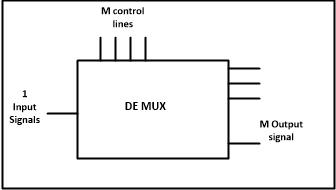
2. Why is a
demultiplexer called a data distributor?
a) The input will be distributed to one of the outputs
b) One of the inputs will be selected for the output
c) The output will be distributed to one of the inputs
d) Single input to Single Output
View
Answer
Answer: a
Explanation: A demultiplexer sends a single input to multiple outputs,
depending on the select lines. For one input, the demultiplexer gives several
outputs. That is why it is called a data distributor.
3. Most demultiplexers
facilitate which type of conversion?
a) Decimal-to-hexadecimal
b) Single input, multiple outputs
c) AC to DC
d) Odd parity to even parity
View
Answer
Answer: b
Explanation: A demultiplexer sends a single input to multiple outputs,
depending on the select lines. Demultiplexer converts single input into
multiple outputs.
Subscribe Now: Digital Electronics Newsletter | Important Subjects Newsletters
advertisement
4. In 1-to-4
demultiplexer, how many select lines are required?
a) 2
b) 3
c) 4
d) 5
View
Answer
Answer: a
Explanation: The formula for total no. of outputs is given by 2n, where n is the no. of select lines. Therefore, for 1:4
demultiplexer, 2 select lines are required.
5. In a multiplexer
the output depends on its ___________
a) Data inputs
b) Select inputs
c) Select outputs
d) Enable pin
View
Answer
Answer: b
Explanation: A demultiplexer sends a single input to multiple outputs,
depending on the select lines. As the select input changes, the output of the
multiplexer varies according to that input.
Participate in Digital Circuits Certification Contest of the Month Now!
6. In 1-to-4
multiplexer, if C1 = 0 & C2 = 1, then the output will be ___________
a) Y0
b) Y1
c) Y2
d) Y3
View
Answer
Answer: b
Explanation: It can be calculated from the figure shown below:

For C0 =1 and C1 =0, Y1 will be the output as 0 and 1 are the bit combinations
of 1.
7. In 1-to-4
multiplexer, if C1 = 1 & C2 = 1, then the output will be ___________
a) Y0
b) Y1
c) Y2
d) Y3
View
Answer
Answer: d
Explanation: It can be calculated from the figure shown below:
For C0 =1 and C1 =0, Y3 will be the output as 0 and 1 are the bit combinations
of 1.
8. How many select
lines are required for a 1-to-8 demultiplexer?
a) 2
b) 3
c) 4
d) 5
View
Answer
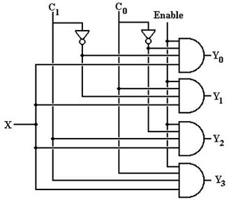
9. How many AND gates
are required for a 1-to-8 multiplexer?
a) 2
b) 6
c) 8
d) 5
View
Answer
Answer: c
Explanation: The number of AND gates required will be equal to the number of
outputs in a demultiplexer, which are 8.
10. The output Q4 of
this 1-to-8 demultiplexer is ____________
a) Q2.(Q1)’.Q0.I
b) Q2.Q1.(Q0)’.I
c) Q2.(Q1)’.(Q0)’.I
d) Q2.(Q1).Q0.I
View
Answer
Answer: c
Explanation: The output Y4 = Q2.(Q1)’.(Q0)’.I. since the bit combinations of 4
are 100.
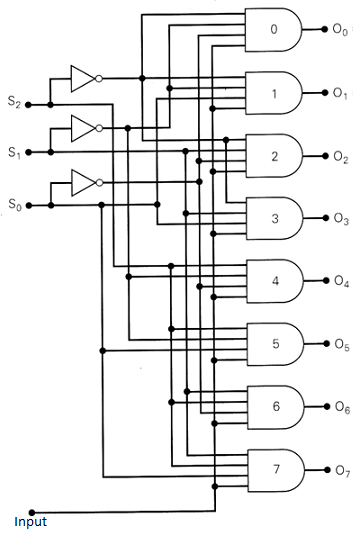
11. Which IC is used
for the implementation of 1-to-16 DEMUX?
a) IC 74154
b) IC 74155
c) IC 74139
d) IC 74138
View
Answer
Answer: a
Explanation: IC 74154 is used for the implementation of 1-to-16 DEMUX, whose
output is inverted input.
1. Why is a
demultiplexer called a data distributor?
a) The input will be distributed to one of the outputs
b) One of the inputs will be selected for the output
c) The output will be distributed to one of the inputs
d) Single input gives single output
View
Answer
Answer: a
Explanation: A demultiplexer sends a single input to multiple outputs,
depending on the select lines. For one input, the demultiplexer gives several
outputs. That is why it is called a data distributor.
2. Most demultiplexers
facilitate which type of conversion?
a) Decimal-to-hexadecimal
b) Single input, multiple outputs
c) AC to DC
d) Odd parity to even parity
View
Answer
Answer: b
Explanation: A demultiplexer sends a single input to multiple outputs,
depending on the select lines. Demultiplexer converts single input into
multiple outputs.
3. In 1-to-4
demultiplexer, how many select lines are required?
a) 2
b) 3
c) 4
d) 5
View
Answer
Answer: a
Explanation: The formula for total no. of outputs is given by 2n, where n is the no. of select lines. Therefore, for 1:4
demultiplexer, 2 select lines are required.
Subscribe Now: Digital Electronics Newsletter | Important Subjects Newsletters
advertisement
4. In a multiplexer
the output depends on its ____________
a) Data inputs
b) Select inputs
c) Select outputs
d) Enable pin
View
Answer
Answer: b
Explanation: A demultiplexer sends a single input to multiple outputs,
depending on the select lines. As the select input changes, the output of the
multiplexer varies according to that input.
5. In 1-to-4
multiplexer, if C1 = 1 & C2 = 1, then the output will be ____________
a) Y0
b) Y1
c) Y2
d) Y3
View
Answer
Answer: d
Explanation: It can be calculated from the figure shown below:
For C0 =1 and C1 =1, Y3 will be the output as 0 and 1 are the bit combinations
of 1.
Participate in Digital Circuits Certification Contest of the Month Now!
6. How many select
lines are required for a 1-to-8 demultiplexer?
a) 2
b) 3
c) 4
d) 5
View
Answer
Answer: b
Explanation: The formula for total no. of outputs is given by 2n, where n is the no. of select lines. In this case n = 3 since 23 = 8.
7. How many AND gates
are required for a 1-to-8 multiplexer?
a) 2
b) 6
c) 8
d) 5
View
Answer
Answer: c
Explanation: The number of AND gates required will be equal to the number of
outputs in a demultiplexer, which are 8.
8. Which IC is used
for the implementation of 1-to-16 DEMUX?
a) IC 74154
b) IC 74155
c) IC 74139
d) IC 74138
View
Answer
Answer: a
Explanation: IC 74154 is used for the implementation of 1-to-16 DEMUX, whose
output is inverted input.
1. How many inputs
will a decimal-to-BCD encoder have?
a) 4
b) 8
c) 10
d) 16
View
Answer
Answer: c
Explanation: An encoder is a combinational circuit encoding the information of
2n input lines to n output lines, thus
producing the binary equivalent of the input. Thus, a Decimal-to-bcd converter
has decimal values as inputs which range from 0-9. So, a total of 10 inputs are
there in a decimal-to-BCD encoder.
2. How many outputs
will a decimal-to-BCD encoder have?
a) 4
b) 8
c) 12
d) 16
View
Answer
Answer: a
Explanation: An encoder is a combinational circuit encoding the information of
2n input lines to n output lines, thus
producing the binary equivalent of the input. Thus, a decimal to BCD encoder
has 4 outputs.
3. How is an encoder
different from a decoder?
a) The output of an encoder is a binary code for 1-of-N input
b) The output of a decoder is a binary code for 1-of-N input
c) The output of an encoder is a binary code for N-of-1 output
d) The output of a decoder is a binary code for N-of-1 output
View
Answer
Answer: a
Explanation: An encoder is a combinational circuit encoding the information of
2n input lines to n output lines, thus
producing the binary equivalent of the input. It performs the opposite
operation of a decoder which results in 2n outputs from n
inputs. Thus, an encoder different from a decoder because of the output of an
encoder is a binary code for 1-of-N input.
Sanfoundry Certification Contest of the Month is Live. 100+ Subjects. Participate Now!
advertisement
4. If we record any
music in any recorder, such types of process is called ___________
a) Multiplexing
b) Encoding
c) Decoding
d) Demultiplexing
View
Answer
Answer: b
Explanation: If we record any music in any recorder, it means that we are
giving data to a recorder. So, such process is called encoding. Getting back
the music from the recorded data is known as decoding.
5. Can an encoder be a
transducer?
a) Yes
b) No
c) May or may not be
d) Both are not even related slightly
View
Answer
Answer: a
Explanation: Of course, a transducer is a device that has the capability to
emit data as well as to accept. Transducer converts signal from one form of
energy to another.
Check this: Digital Electronics Books | Electronics & Communication Engineering Books
6. How many OR gates
are required for a Decimal-to-bcd encoder?
a) 2
b) 10
c) 3
d) 4
View
Answer
Answer: d
Explanation: An encoder is a combinational circuit encoding the information of
2^n input lines to n output lines, thus producing the binary equivalent of the
input.
This is clear from the diagram that it requires 4 OR gates:
 .
.
7. How many OR gates
are required for an octal-to-binary encoder?
a) 3
b) 2
c) 8
d) 10
View
Answer
Answer: a
Explanation: An encoder is a combinational circuit encoding the information of
2n input lines to n output lines, thus
producing the binary equivalent of the input. Thus, in octal to binary encoder
there are 8 (=23) inputs, thus 3 output lines.
8. For 8-bit input
encoder how many combinations are possible?
a) 8
b) 2^8
c) 4
d) 2^4
View
Answer
Answer: b
Explanation: An encoder is a combinational circuit encoding the information of
2n input lines to n output lines, thus
producing the binary equivalent of the input. There are 28 combinations are possible for an 8-bit input encoder but
out of which only 8 are used using 3 output lines. It is a disadvantage of
encoder.
9. The discrepancy of
0 output due to all inputs being 0 or D0, being 0 is resolved by using
additional input known as ___________
a) Enable
b) Disable
c) Strobe
d) Clock
View
Answer
Answer: a
Explanation: Such problems are resolved by using enable input, which behaves as
active if it gets 0 as input since it is an active-low pin.
10. Can an encoder be
called a multiplexer?
a) No
b) Yes
c) Sometimes
d) Never
View
Answer
Answer: b
Explanation: A multiplexer or MUX is a combination circuit that contains more
than one input line, one output line and more than one selection line. Whereas,
an encoder is also considered a type of multiplexer but without a single output
line and without any selection lines.
11. If two inputs are
active on a priority encoder, which will be coded on the output?
a) The higher value
b) The lower value
c) Neither of the inputs
d) Both of the inputs
View
Answer
Answer: a
Explanation: An encoder is a combinational circuit encoding the information of
2n input lines to n output lines, thus
producing the binary equivalent of the input. If two inputs are active on a
priority encoder, the input of higher value will be coded in the output.
Unit 4
1. Latches constructed
with NOR and NAND gates tend to remain in the latched condition due to which
configuration feature?
a) Low input voltages
b) Synchronous operation
c) Gate impedance
d) Cross coupling
View
Answer
Answer: d
Explanation: Latch is a type of bistable multivibrator having two stable
states. Both inputs of a latch are directly connected to the other’s output.
Such types of structure is called cross coupling and due to which latches
remain in the latched condition.
2. One example of the
use of an S-R flip-flop is as ___________
a) Transition pulse generator
b) Racer
c) Switch debouncer
d) Astable oscillator
View
Answer
Answer: c
Explanation: The SR flip-flop is very effective in removing the effects of
switch bounce, which is the unwanted noise caused during the switching of
electronic devices.
3. The truth table for
an S-R flip-flop has how many VALID entries?
a) 1
b) 2
c) 3
d) 4
View
Answer
Answer: c
Explanation: The SR flip-flop actually has three inputs, Set, Reset and its
current state. The Invalid or Undefined State occurs at both S and R being at
1.
Note: Join free Sanfoundry classes at Telegram or Youtube
advertisement
4. When both inputs of
a J-K flip-flop cycle, the output will ___________
a) Be invalid
b) Change
c) Not change
d) Toggle
View
Answer
Answer: c
Explanation: After one cycle the value of each input comes to the same value.
Eg: Assume J=0 and K=1. After 1 cycle, it becomes as J=0->1->0(1 cycle
complete) and K=1->0->1(1 cycle complete). The J & K flip-flop has 4
stable states: Latch, Reset, Set and Toggle.
5. Which of the
following is correct for a gated D-type flip-flop?
a) The Q output is either SET or RESET as soon as the D input goes HIGH or LOW
b) The output complement follows the input when enabled
c) Only one of the inputs can be HIGH at a time
d) The output toggles if one of the inputs is held HIGH
View
Answer
Answer: a
Explanation: In D flip flop, when the clock is high then the output depends on
the input otherwise reminds previous output. In a state of clock high, when D
is high the output Q also high, if D is ‘0’ then output is also zero. Like SR
flip-flop, the D-flip-flop also have an invalid state at both inputs being 1.
Take Digital Circuits Practice Tests -
Chapterwise!
Start the Test Now: Chapter 1, 2, 3, 4, 5, 6, 7, 8, 9, 10
6. A basic S-R
flip-flop can be constructed by cross-coupling of which basic logic gates?
a) AND or OR gates
b) XOR or XNOR gates
c) NOR or NAND gates
d) AND or NOR gates
View
Answer
Answer: c
Explanation: The basic S-R flip-flop can be constructed by cross coupling of
NOR or NAND gates. Cross coupling means the output of second gate is fed to the
input of first gate and vice-versa.
7. The logic circuits
whose outputs at any instant of time depends only on the present input but also
on the past outputs are called ________________
a) Combinational circuits
b) Sequential circuits
c) Latches
d) Flip-flops
View
Answer
Answer: b
Explanation: In sequential circuits, the output signals are fed back to the
input side. So, The circuits whose outputs at any instant of time depends only
on the present input but also on the past outputs are called sequential
circuits. Unlike sequential circuits, if output depends only on the present
state, then it’s known as combinational circuits.
8. Whose operations
are more faster among the following?
a) Combinational circuits
b) Sequential circuits
c) Latches
d) Flip-flops
View
Answer
Answer: a
Explanation: Combinational circuits are often faster than sequential circuits.
Since the combinational circuits do not require memory elements whereas the
sequential circuits need memory devices to perform their operations in
sequence. Latches and Flip-flops come under sequential circuits.
9. How many types of
sequential circuits are?
a) 2
b) 3
c) 4
d) 5
View
Answer
Answer: a
Explanation: There are two type of sequential circuits viz., (i) synchronous or
clocked and (ii) asynchronous or unclocked. Synchronous Sequential Circuits are
triggered in the presence of a clock signal, whereas, Asynchronous Sequential
Circuits function in the absence of a clock signal.
10. The sequential
circuit is also called ___________
a) Flip-flop
b) Latch
c) Strobe
d) Adder
View
Answer
Answer: b
Explanation: The sequential circuit is also called a latch because both are a
memory cell, which are capable of storing one bit of information.
11. The basic latch
consists of ___________
a) Two inverters
b) Two comparators
c) Two amplifiers
d) Two adders
View
Answer
Answer: a
Explanation: The basic latch consists of two inverters. It is in the sense that
if the output Q = 0 then the second output Q’ = 1 and vice versa.
12. In S-R flip-flop,
if Q = 0 the output is said to be ___________
a) Set
b) Reset
c) Previous state
d) Current state
View
Answer
Answer: b
Explanation: In S-R flip-flop, if Q = 0 the output is said to be reset and set
for Q = 1.
13. The output of
latches will remain in set/reset untill ___________
a) The trigger pulse is given to change the state
b) Any pulse given to go into previous state
c) They don’t get any pulse more
d) The pulse is edge-triggered
View
Answer
Answer: a
Explanation: The output of latches will remain in set/reset untill the trigger
pulse is given to change the state.
14. What is a trigger
pulse?
a) A pulse that starts a cycle of operation
b) A pulse that reverses the cycle of operation
c) A pulse that prevents a cycle of operation
d) A pulse that enhances a cycle of operation
View
Answer
Answer: a
Explanation: Trigger pulse is defined as a pulse that starts a cycle of
operation.
15. The circuits of
NOR based S-R latch classified as asynchronous sequential circuits, why?
a) Because of inverted outputs
b) Because of triggering functionality
c) Because of cross-coupled connection
d) Because of inverted outputs & triggering functionality
View
Answer
Answer: c
Explanation: The cross-coupled connections from the output of one gate to the
input of the other gate constitute a feedback path. For this reason, the
circuits of NOR based S-R latch classified as asynchronous sequential circuits.
Moreover, they are referred to as asynchronous because they function in the
absence of a clock pulse.
1. What is an
ambiguous condition in a NAND based S’-R’ latch?
a) S’=0, R’=1
b) S’=1, R’=0
c) S’=1, R’=1
d) S’=0, R’=0
View
Answer
Answer: d
Explanation: In a NAND based S-R latch, If S’=0 & R’=0 then both the
outputs (i.e. Q & Q’) goes HIGH and this condition is called an
ambiguous/forbidden state. This state is also known as an Invalid state as the
system goes into an unexpected situation.
2. In a NAND based
S’-R’ latch, if S’=1 & R’=1 then the state of the latch is ____________
a) No change
b) Set
c) Reset
d) Forbidden
View
Answer
Answer: a
Explanation: In a NAND based S’-R, latch if S’=1 & R’=1 then there is no
any change in the state. It remains in its prior state. This state is used for
the storage of data.
3. A NAND based S’-R’
latch can be converted into S-R latch by placing ____________
a) A D latch at each of its input
b) An inverter at each of its input
c) It can never be converted
d) Both a D latch and an inverter at its input
View
Answer
Answer: d
Explanation: A NAND based S’-R’ latch can be converted into S-R latch by
placing either a D latch or an inverter at its input as it’s operations will be
complementary.
Note: Join free Sanfoundry classes at Telegram or Youtube
advertisement
4. One major
difference between a NAND based S’-R’ latch & a NOR based S-R latch is
____________
a) The inputs of NOR latch are 0 but 1 for NAND latch
b) The inputs of NOR latch are 1 but 0 for NAND latch
c) The output of NAND latch becomes set if S’=0 & R’=1 and vice versa for
NOR latch
d) The output of NOR latch is 1 but 0 for NAND latch
View
Answer
Answer: a
Explanation: Due to inverted input of NAND based S’-R’ latch, the inputs of NOR
latch are 0 but 1 for NAND latch.
5. The characteristic
equation of S-R latch is ____________
a) Q(n+1) = (S + Q(n))R’
b) Q(n+1) = SR + Q(n)R
c) Q(n+1) = S’R + Q(n)R
d) Q(n+1) = S’R + Q'(n)R
View
Answer
Answer: a
Explanation: A characteristic equation is needed when a specific gate requires
a specific output in order to satisfy the truth table. The characteristic
equation of S-R latch is Q(n+1) = (S + Q(n))R’.
Take Digital Circuits Mock Tests -
Chapterwise!
Start the Test Now: Chapter 1, 2, 3, 4, 5, 6, 7, 8, 9, 10
6. The difference
between a flip-flop & latch is ____________
a) Both are same
b) Flip-flop consist of an extra output
c) Latches has one input but flip-flop has two
d) Latch has two inputs but flip-flop has one
View
Answer
Answer: c
Explanation: Flip-flop is a modified version of latch. To determine the changes
in states, an additional control input is provided to the latch.
7. How many types of
flip-flops are?
a) 2
b) 3
c) 4
d) 5
View
Answer
Answer: c
Explanation: There are 4 types of flip-flops, viz., S-R, J-K, D, and T. D
flip-flop is an advanced version of S-R flip-flop, while T flip-flop is an
advanced version of J-K flip-flop.
8. The S-R flip flop
consist of ____________
a) 4 AND gates
b) Two additional AND gates
c) An additional clock input
d) 3 AND gates
View
Answer
Answer: b
Explanation: The S-R flip flop consists of two additional AND gates at the S
and R inputs of S-R latch.
9. What is one
disadvantage of an S-R flip-flop?
a) It has no Enable input
b) It has a RACE condition
c) It has no clock input
d) Invalid State
View
Answer
Answer: d
Explanation: The main drawback of s-r flip flop is invalid output when both the
inputs are high, which is referred to as Invalid State.
10. One example of the
use of an S-R flip-flop is as ____________
a) Racer
b) Stable oscillator
c) Binary storage register
d) Transition pulse generator
View
Answer
Answer: c
Explanation: S-R refers to set-reset. So, it is used to store two values 0 and
1. Hence, it is referred to as binary storage element. It functions as memory
storage during the No Change State.
11. When is a
flip-flop said to be transparent?
a) When the Q output is opposite the input
b) When the Q output follows the input
c) When you can see through the IC packaging
d) When the Q output is complementary of the input
View
Answer
Answer: b
Explanation: Flip-flop have the property of responding immediately to the
changes in its inputs. This property is called transparency.
12. On a positive
edge-triggered S-R flip-flop, the outputs reflect the input condition when
________
a) The clock pulse is LOW
b) The clock pulse is HIGH
c) The clock pulse transitions from LOW to HIGH
d) The clock pulse transitions from HIGH to LOW
View
Answer
Answer: c
Explanation: Edge triggered device will follow when there is transition. It is
a positive edge triggered when transition takes place from low to high, while,
it is negative edge triggered when the transition takes place from high to low.
13. What is the hold
condition of a flip-flop?
a) Both S and R inputs activated
b) No active S or R input
c) Only S is active
d) Only R is active
View
Answer
Answer: b
Explanation: The hold condition in a flip-flop is obtained when both of the
inputs are LOW. It is the No Change State or Memory Storage state if a
flip-flop.
14. If an active-HIGH
S-R latch has a 0 on the S input and a 1 on the R input and then the R input
goes to 0, the latch will be ________
a) SET
b) RESET
c) Clear
d) Invalid
View
Answer
Answer: b
Explanation: If S=0, R=1, the flip flop is at reset condition. Then at S=0, R=0,
there is no change. So, it remains in reset. If S=1, R=0, the flip flop is at
the set condition.
15. The circuit that
is primarily responsible for certain flip-flops to be designated as
edge-triggered is the _____________
a) Edge-detection circuit
b) NOR latch
c) NAND latch
d) Pulse-steering circuit
View
Answer
Answer: a
Explanation: The circuit that is primarily responsible for certain flip-flops
to be designated as edge-triggered is the edge-detection circuit.
1. Which circuit is
generated from D flip-flop due to addition of an inverter by causing reduction
in the number of inputs?
a) Gated JK-latch
b) Gated SR-latch
c) Gated T-latch
d) Gated D-latch
View
Answer
Answer: d
Explanation: Since, both inputs of the D flip-flop are connected through an inverter.
And this causes reduction in the number of inputs.
2. The characteristic
of J-K flip-flop is similar to _____________
a) S-R flip-flop
b) D flip-flop
c) T flip-flop
d) Gated T flip-flop
View
Answer
Answer: a
Explanation: In an S-R flip-flop, S refers to “SET” whereas R refers to
“RESET”. The same behaviour is shown by J-K flip-flop.
3. A J-K flip-flop can
be obtained from the clocked S-R flip-flop by augmenting ___________
a) Two AND gates
b) Two NAND gates
c) Two NOT gates
d) Two OR gates
View
Answer
Answer: a
Explanation: A J-K flip-flop can be obtained from the clocked S-R flip-flop by
augmenting two AND gates.
Subscribe Now: Digital Electronics Newsletter | Important Subjects Newsletters
advertisement
4. How is a J-K
flip-flop made to toggle?
a) J = 0, K = 0
b) J = 1, K = 0
c) J = 0, K = 1
d) J = 1, K = 1
View
Answer
Answer: d
Explanation: When j=k=1 then the race condition is occurs that means both
output wants to be HIGH. Hence, there is toggle condition is occurs, where 0
becomes 1 and 1 becomes 0. That is device is either set or reset.
5. The phenomenon of
interpreting unwanted signals on J and K while Cp (clock pulse) is HIGH is
called ___________
a) Parity error checking
b) Ones catching
c) Digital discrimination
d) Digital filtering
View
Answer
Answer: b
Explanation: Ones catching means that the input transitioned to a 1 and back
very briefly (unintentionally due to a glitch), but the flip-flop responded and
latched it in anyway, i.e., it caught the 1. Similarly for 0’s catching.
Participate in Digital Circuits Certification Contest of the Month Now!
6. In J-K flip-flop,
“no change” condition appears when ___________
a) J = 1, K = 1
b) J = 1, K = 0
c) J = 0, K = 1
d) J = 0, K = 0
View
Answer
Answer: d
Explanation: If J = 0, K = 0, the output remains unchanged. This is the memory
storing state.
7. A J-K flip-flop
with J = 1 and K = 1 has a 20 kHz clock input. The Q output is ________
a) Constantly LOW
b) Constantly HIGH
c) A 20 kHz square wave
d) A 10 kHz square wave
View
Answer
Answer: d
Explanation: The flip flop is sensitive only to the positive or negative edge
of the clock pulse. So, the flip-flop toggles whenever the clock is
falling/rising at edge. This triggering of flip-flop during the transition
state, is known as Edge-triggered flip-flop. Thus, the output curve has a time
period twice that of the clock. Frequency is inversely related to time period
and hence frequency gets halved.
8. What is the
significance of the J and K terminals on the J-K flip-flop?
a) There is no known significance in their designations
b) The J represents “jump,” which is how the Q output reacts whenever the clock
goes high and the J input is also HIGH
c) The letters were chosen in honour of Jack Kilby, the inventory of the
integrated circuit
d) All of the other letters of the alphabet are already in use
View
Answer
Answer: c
Explanation: The letters J & K were chosen in honour of Jack Kilby, the
inventory of the integrated circuit. In J&K flip-flops, the invalid state
problem is resolved, thus leading to the toggling of states.
9. On a J-K flip-flop,
when is the flip-flop in a hold condition?
a) J = 0, K = 0
b) J = 1, K = 0
c) J = 0, K = 1
d) J = 1, K = 1
View
Answer
Answer: a
Explanation: At J=0 k=0 output continues to be in the same state. This is the
memory storing state.
10. Two J-K flip-flops
with their J-K inputs tied HIGH are cascaded to be used as counters. After four
input clock pulses, the binary count is ________
a) 00
b) 11
c) 01
d) 10
View
Answer
Answer: a
Explanation: Every O/P repeats after its mod. Here mod is 4 (because 2
flip-flops are used. So mod = 22 = 4). So after 4
clock pulses the O/P repeats i.e. 00.
11. Four J-K
flip-flops are cascaded with their J-K inputs tied HIGH. If the input frequency
(fin) to the first flip-flop is 32 kHz, the output frequency (fout) is ________
a) 1 kHz
b) 2 kHz
c) 4 kHz
d) 16 kHz
View
Answer
Answer: b
Explanation: 32/2=16:-first flip-flop, 16/2=8:- second flip-flop, 8/2=4:- third
flip-flop, 4/2=2:- fourth flip-flop. Since the output frequency is determined
on basis of the 4th flip-flop.
12. Determine the
output frequency for a frequency division circuit that contains 12 flip-flops
with an input clock frequency of 20.48 MHz.
a) 10.24 kHz
b) 5 kHz
c) 30.24 kHz
d) 15 kHz
View
Answer
Answer: b
Explanation: 12 flip flops = 212 = 4096
Input Clock frequency = 20.48*106 = 20480000
Output Clock frequency = 20480000/4096 = 5000 i.e., 5 kHz.
13. How many
flip-flops are in the 7475 IC?
a) 2
b) 1
c) 4
d) 8
View
Answer
Answer: c
Explanation: There are 4 flip-flops used in 7475 IC and those are D flip-flops
only.
1. In D flip-flop, D
stands for _____________
a) Distant
b) Data
c) Desired
d) Delay
View
Answer
Answer: b
Explanation: The D of D-flip-flop stands for “data”. It stores the value on the
data line.
2. The D flip-flop has
_______ input.
a) 1
b) 2
c) 3
d) 4
View
Answer
Answer: a
Explanation: The D flip-flop has one input. The D of D-flip-flop stands for
“data”. It stores the value on the data line.
3. The D flip-flop has
______ output/outputs.
a) 2
b) 3
c) 4
d) 1
View
Answer
Answer: a
Explanation: The D flip-flop has two outputs: Q and Q complement. The D
flip-flop has one input. The D of D-flip-flop stands for “data”. It stores the
value on the data line.
Sanfoundry Certification Contest of the Month is Live. 100+ Subjects. Participate Now!
advertisement
4. A D flip-flop can
be constructed from an ______ flip-flop.
a) S-R
b) J-K
c) T
d) S-K
View
Answer
Answer: a
Explanation: A D flip-flop can be constructed from an S-R flip-flop by
inserting an inverter between S and R and assigning the symbol D to the S
input.
5. In D flip-flop, if
clock input is LOW, the D input ___________
a) Has no effect
b) Goes high
c) Goes low
d) Has effect
View
Answer
Answer: a
Explanation: In D flip-flop, if clock input is LOW, the D input has no effect,
since the set and reset inputs of the NAND flip-flop are kept HIGH.
Check this: Electrical Engineering Books | Electrical Engineering MCQs
6. In D flip-flop, if
clock input is HIGH & D=1, then output is ___________
a) 0
b) 1
c) Forbidden
d) Toggle
View
Answer
Answer: a
Explanation: If clock input is HIGH & D=1, then output is 0. It can be
observed from this diagram:
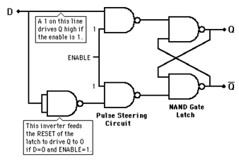
7. Which statement
describes the BEST operation of a negative-edge-triggered D flip-flop?
a) The logic level at the D input is transferred to Q on NGT of CLK
b) The Q output is ALWAYS identical to the CLK input if the D input is HIGH
c) The Q output is ALWAYS identical to the D input when CLK = PGT
d) The Q output is ALWAYS identical to the D input
View
Answer
Answer: a
Explanation: By the truth table of D flip flop, we can observe that Q always
depends on D. Hence, for every negative trigger pulse, the logic at input D is
shifted to Output Q.
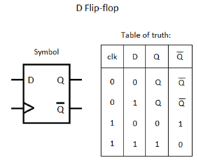
8. Which of the
following is correct for a gated D flip-flop?
a) The output toggles if one of the inputs is held HIGH
b) Only one of the inputs can be HIGH at a time
c) The output complement follows the input when enabled
d) Q output follows the input D when the enable is HIGH
View
Answer
Answer: d
Explanation: If clock is high then the D flip-flop operate and we know that
input is equals to output in case of D flip-flop. It stores the value on the
data line.
9. With regard to a D
latch ________
a) The Q output follows the D input when EN is LOW
b) The Q output is opposite the D input when EN is LOW
c) The Q output follows the D input when EN is HIGH
d) The Q output is HIGH regardless of EN’s input state
View
Answer
Answer: c
Explanation: Latch is nothing but flip flop which holds the o/p or i/p state.
And in D flip-flop output follows the input. It stores the value on the data
line.
10. Which of the
following is correct for a D latch?
a) The output toggles if one of the inputs is held HIGH
b) Q output follows the input D when the enable is HIGH
c) Only one of the inputs can be HIGH at a time
d) The output complement follows the input when enabled
View
Answer
Answer: b
Explanation: If the clock is HIGH then the D flip-flop operates and we know
that input equals to output in case of D flip flop. It stores the value on the
data line.
11. Which of the
following describes the operation of a positive edge-triggered D flip-flop?
a) If both inputs are HIGH, the output will toggle
b) The output will follow the input on the leading edge of the clock
c) When both inputs are LOW, an invalid state exists
d) The input is toggled into the flip-flop on the leading edge of the clock and
is passed to the output on the trailing edge of the clock
View
Answer
Answer: b
Explanation: Edge-triggered flip-flop means the device will change state during
the rising or falling edge of the clock pulse. The main phenomenon of the D
flip-flop is that the o/p will follow the i/p when the enable pin is HIGH.
12. A D flip-flop
utilizing a PGT clock is in the CLEAR state. Which of the following input
actions will cause it to change states?
a) CLK = NGT, D = 0
b) CLK = PGT, D = 0
c) CLOCK NGT, D = 1
d) CLOCK PGT, D = 1
View
Answer
Answer: d
Explanation: PGT refers to Positive Going Transition and NGT refers to negative
Going Transition. Earlier, the DFF is in a clear state (output is 0). So, if D
= 1 then in the next stage output will be 1 and hence the stage will be
changed.
13. A positive
edge-triggered D flip-flop will store a 1 when ________
a) The D input is HIGH and the clock transitions from HIGH to LOW
b) The D input is HIGH and the clock transitions from LOW to HIGH
c) The D input is HIGH and the clock is LOW
d) The D input is HIGH and the clock is HIGH
View
Answer
Answer: b
Explanation: A positive edge-triggered D flip-flop will store a 1 when the D
input is HIGH and the clock transitions from LOW to HIGH. While a negative
edge-triggered D flip-flop will store a 0 when the D input is HIGH and the
clock transitions from HIGH to LOW.
14. Why do the D
flip-flops receive its designation or nomenclature as ‘Data Flip-flops’?
a) Due to its capability to receive data from flip-flop
b) Due to its capability to store data in flip-flop
c) Due to its capability to transfer the data into flip-flop
d) Due to erasing the data from the flip-flop
View
Answer
Answer: c
Explanation: Due to its capability to transfer the data into flip-flop.
D-flip-flops stores the value on the data line.
15. The characteristic
equation of D-flip-flop implies that ___________
a) The next state is dependent on previous state
b) The next state is dependent on present state
c) The next state is independent of previous state
d) The next state is independent of present state
View
Answer
Answer: d
Explanation: A characteristic equation is needed when a specific gate requires
a specific output in order to satisfy the truth table. The characteristic
equation of D flip-flop is given by Q(n+1) = D; which indicates that the next state
is independent of the present state
1. The characteristic
equation of J-K flip-flop is ______________
a) Q(n+1)=JQ(n)+K’Q(n)
b) Q(n+1)=J’Q(n)+KQ'(n)
c) Q(n+1)=JQ'(n)+KQ(n)
d) Q(n+1)=JQ'(n)+K’Q(n)
View
Answer
Answer: d
Explanation: A characteristic equation is needed when a specific gate requires
a specific output in order to satisfy the truth table. The characteristic
equation of J-K flip-flop is given by: Q(n+1)=JQ'(n)+K’Q(n).
2. In a J-K flip-flop,
if J=K the resulting flip-flop is referred to as _____________
a) D flip-flop
b) S-R flip-flop
c) T flip-flop
d) S-K flip-flop
View
Answer
Answer: c
Explanation: In J-K flip-flop, if both the inputs are same then it behaves like
T flip-flop.
3. In J-K flip-flop,
the function K=J is used to realize _____________
a) D flip-flop
b) S-R flip-flop
c) T flip-flop
d) S-K flip-flop
View
Answer
Answer: c
Explanation: T flip-flop allows the same inputs. So, in J-K flip-flop J=K then
it will work as T flip-flop.
Note: Join free Sanfoundry classes at Telegram or Youtube
advertisement
4. The only difference
between a combinational circuit and a flip-flop is that _____________
a) The flip-flop requires previous state
b) The flip-flop requires next state
c) The flip-flop requires a clock pulse
d) The flip-flop depends on the past as well as present states
View
Answer
Answer: c
Explanation: Both flip-flop and latches are memory elements with clock/control
inputs. They depend on the past as well as present states. Whereas, in case of
combinational circuits, they only depend on the present state.
5. How many stable
states combinational circuits have?
a) 3
b) 4
c) 2
d) 5
View
Answer
Answer: c
Explanation: The two stable states of combinational circuits are 1 and 0.
Whereas, in flip-flops there is an additional state known as Forbidden State.
Take Digital Circuits Mock Tests -
Chapterwise!
Start the Test Now: Chapter 1, 2, 3, 4, 5, 6, 7, 8, 9, 10
6. The flip-flop is
only activated by _____________
a) Positive edge trigger
b) Negative edge trigger
c) Either positive or Negative edge trigger
d) Sinusoidal trigger
View
Answer
Answer: c
Explanation: Flip flops can be activated with either a positive or negative
edge trigger.
7. The S-R latch
composed of NAND gates is called an active low circuit because _____________
a) It is only activated by a positive level trigger
b) It is only activated by a negative level trigger
c) It is only activated by either a positive or negative level trigger
d) It is only activated by sinusoidal trigger
View
Answer
Answer: b
Explanation: Active low indicates that only an input value of 0 sets or resets
the circuit.
8. Both the J-K &
the T flip-flop are derived from the basic _____________
a) S-R flip-flop
b) S-R latch
c) D latch
d) D flip-flop
View
Answer
Answer: b
Explanation: The SR latch is the basic block for the D latch/flip flop from
which the JK and T flip flops are derived. A latch is similar to a flip-flop,
only without a clock input.
9. The flip-flops
which has not any invalid states are _____________
a) S-R, J-K, D
b) S-R, J-K, T
c) J-K, D, S-R
d) J-K, D, T
View
Answer
Answer: d
Explanation: Unlike the SR latch, these circuits have no invalid states. The SR
latch or flip-flop has an invalid or forbidden state where no output could be
determined.
10. What does the
triangle on the clock input of a J-K flip-flop mean?
a) Level enabled
b) Edge triggered
c) Both Level enabled & Edge triggered
d) Level triggered
View
Answer
Answer: b
Explanation: The triangle on the clock input of a J-K flip-flop mean edge
triggered. Whereas the absence of triangle symbol implies that the flip-flop is
level-triggered.
11. What does the
circle on the clock input of a J-K flip-flop mean?
a) Level enabled
b) Positive edge triggered
c) negative edge triggered
d) Level triggered
View
Answer
Answer: c
Explanation: The circle on the clock input of a J-K flip-flop mean negative
edge triggered. Whereas the absence of triangle symbol implies that the
flip-flop is level-triggered.
12. What does the
direct line on the clock input of a J-K flip-flop mean?
a) Level enabled
b) Positive edge triggered
c) negative edge triggered
d) Level triggered
View
Answer
Answer: d
Explanation: The direct line on the clock input of a J-K flip-flop mean level
triggered. Whereas the presence of triangle symbol implies that the flip-flop
is edge-triggered.
13. What does the half
circle on the clock input of a J-K flip-flop mean?
a) Level enabled
b) Positive edge triggered
c) negative edge triggered
d) Level triggered
View
Answer
Answer: d
Explanation: The half circle on the clock input of a J-K flip-flop mean level
triggered. Whereas the presence of triangle symbol implies that the flip-flop
is edge-triggered.
14. A J-K flip-flop
with J = 1 and K = 1 has a 20 kHz clock input. The Q output is _____________
a) Constantly LOW
b) Constantly HIGH
c) A 20 kHz square wave
d) A 10 kHz square wave
View
Answer
Answer: d
Explanation: As one flip flop is used so there are two states available. So,
20/2 = 10Hz frequency is available at the output.
15. On a positive edge-triggered
S-R flip-flop, the outputs reflect the input condition when ________
a) The clock pulse is LOW
b) The clock pulse is HIGH
c) The clock pulse transitions from LOW to HIGH
d) The clock pulse transitions from HIGH to LOW
View
Answer
Answer: c
Explanation: Edge triggered device will follow the input condition when there
is a transition. It is said to be positive edge triggered when transition
occurs from LOW to HIGH. While it is said to be a negative edge triggered when
a transition occurs from HIGH to LOW.
1. The asynchronous
input can be used to set the flip-flop to the ____________
a) 1 state
b) 0 state
c) either 1 or 0 state
d) forbidden State
View
Answer
Answer: c
Explanation: The asynchronous input can be used to set the flip-flop to the 1 state
or clear the flip-flop to the 0 state at any time, regardless of the condition
at the other inputs.
2. Input clock of RS
flip-flop is given to ____________
a) Input
b) Pulser
c) Output
d) Master slave flip-flop
View
Answer
Answer: b
Explanation: Pulser behaves like an arithmetic operator, to perform the
operation or determination of corresponding states.
3. D flip-flop is a
circuit having ____________
a) 2 NAND gates
b) 3 NAND gates
c) 4 NAND gates
d) 5 NAND gates
View
Answer
Answer: c
Explanation: D flip-flop is a circuit having 4 NAND gates. Two of them are
connected with each other.
Subscribe Now: Digital Electronics Newsletter | Important Subjects Newsletters
advertisement
4. In JK flip flop
same input, i.e. at a particular time or during a clock pulse, the output will
oscillate back and forth between 0 and 1. At the end of the clock pulse the
value of output Q is uncertain. The situation is referred to as?
a) Conversion condition
b) Race around condition
c) Lock out state
d) Forbidden State
View
Answer
Answer: b
Explanation: A race around condition is a flaw in an electronic system or
process whereby the output and result of the process is unexpectedly dependent
on the sequence or timing of other events.
5. Master slave flip
flop is also referred to as?
a) Level triggered flip flop
b) Pulse triggered flip flop
c) Edge triggered flip flop
d) Edge-Level triggered flip flop
View
Answer
Answer: b
Explanation: The term pulse triggered means the data is entered on the rising
edge of the clock pulse, but the output does not reflect the change until the
falling edge of the clock pulse.
Become Top Ranker in Digital Circuits Now!
6. In a positive edge
triggered JK flip flop, a low J and low K produces?
a) High state
b) Low state
c) Toggle state
d) No Change State
View
Answer
Answer: d
Explanation: In JK Flip Flop if J = K = 0 then it holds its current state.
There will be no change.
7. If one wants to
design a binary counter, the preferred type of flip-flop is ____________
a) D type
b) S-R type
c) Latch
d) J-K type
View
Answer
Answer: d
Explanation: If one wants to design a binary counter, the preferred type of
flip-flop is J-K type because it has capability to recover from toggle
condition. SR flip-flop is not suitable as it produces the “Invalid State”.
8. S-R type flip-flop
can be converted into D type flip-flop if S is connected to R through
____________
a) OR Gate
b) AND Gate
c) Inverter
d) Full Adder
View
Answer
Answer: c
Explanation: S-R type flip-flop can be converted into D type flip-flop if S is
connected to R through an Inverter gate.
9. Which of the
following flip-flops is free from the race around the problem?
a) T flip-flop
b) SR flip-flop
c) Master-Slave Flip-flop
d) D flip-flop
View
Answer
Answer: a
Explanation: T flip-flop is free from the race around condition because its
output depends only on the input; hence there is no any problem creates as like
toggle.
10. Which of the
following is the Universal Flip-flop?
a) S-R flip-flop
b) J-K flip-flop
c) Master slave flip-flop
d) D Flip-flop
View
Answer
Answer: b
Explanation: There are lots of flip-flops can be prepared by using J-K
flip-flop. So, the name is a universal flip-flop. Also, the JK flip-flop
resolves the Forbidden State.
11. How many types of
triggering take place in a flip flops?
a) 3
b) 2
c) 4
d) 5
View
Answer
Answer: a
Explanation: There are three types of triggering in a flip-flop, viz., level
triggering, edge triggering and pulse triggering.
12. Flip-flops are
____________
a) Stable devices
b) Astable devices
c) Bistable devices
d) Monostable devices
View
Answer
Answer: c
Explanation: Flip-flops are synchronous bistable devices known as bistable
multivibrators as they have 2 stable states.
13. The term
synchronous means ____________
a) The output changes state only when any of the input is triggered
b) The output changes state only when the clock input is triggered
c) The output changes state only when the input is reversed
d) The output changes state only when the input follows it
View
Answer
14. The S-R, J-K and D
inputs are called ____________
a) Asynchronous inputs
b) Synchronous inputs
c) Bidirectional inputs
d) Unidirectional inputs
View
Answer
Answer: b
Explanation: The S-R, J-K and D inputs are called synchronous inputs because
data on these inputs are transferred to the flip-flop’s output only on the
triggering edge or level triggering of the clock pulse. Moreover, flip-flops
have a clock input whereas latches don’t. Hence, known as synchronous inputs.
15. The circuit that
generates a spike in response to a momentary change of input signal is called
____________
a) R-C differentiator circuit
b) L-R differentiator circuit
c) R-C integrator circuit
d) L-R integrator circuit
View
Answer
Answer: a
Explanation: The circuit that generates a spike in response to a momentary
change of input signal is called R-C differentiator circuit.
1. In digital logic, a
counter is a device which ____________
a) Counts the number of outputs
b) Stores the number of times a particular event or process has occurred
c) Stores the number of times a clock pulse rises and falls
d) Counts the number of inputs
View
Answer
Answer: b
Explanation: In digital logic and computing, a counter is a device which stores
(and sometimes displays) the number of times a particular event or process has
occurred, often in relationship to a clock signal.
2. A counter circuit
is usually constructed of ____________
a) A number of latches connected in cascade form
b) A number of NAND gates connected in cascade form
c) A number of flip-flops connected in cascade
d) A number of NOR gates connected in cascade form
View
Answer
Answer: c
Explanation: A counter circuit is usually constructed of a number of flip-flops
connected in cascade. Preferably, JK Flip-flops are used to construct counters
and registers.
3. What is the maximum
possible range of bit-count specifically in n-bit binary counter consisting of
‘n’ number of flip-flops?
a) 0 to 2n
b) 0 to 2n + 1
c) 0 to 2n – 1
d) 0 to 2n+1/2
View
Answer
Answer: c
Explanation: The maximum possible range of bit-count specifically in n-bit
binary counter consisting of ‘n’ number of flip-flops is 0 to 2n-1. For say, there is a 2-bit counter, then it will count till 22-1 = 3. Thus, it will count from 0 to 3.
Sanfoundry Certification Contest of the Month is Live. 100+ Subjects. Participate Now!
advertisement
4. How many types of
the counter are there?
a) 2
b) 3
c) 4
d) 5
View
Answer
Answer: b
Explanation: Counters are of 3 types, namely, (i)asynchronous/synchronous,
(ii)single and multi-mode & (iii)modulus counter. These further can be
subdivided into Ring Counter, Johnson Counter, Cascade Counter, Up/Down Counter
and such like.
5. A decimal counter
has ______ states.
a) 5
b) 10
c) 15
d) 20
View
Answer
Answer: b
Explanation: Decimal counter is also known as 10 stage counter. So, it has 10
states. It is also known as Decade Counter counting from 0 to 9.
Check this: Electrical Engineering MCQs | Electrical Engineering Books
6. Ripple counters are
also called ____________
a) SSI counters
b) Asynchronous counters
c) Synchronous counters
d) VLSI counters
View
Answer
Answer: b
Explanation: Ripple counters are also called asynchronous counter. In
Asynchronous counters, only the first flip-flop is connected to an external
clock while the rest of the flip-flops have their preceding flip-flop output as
clock to them.
7. Synchronous counter
is a type of ____________
a) SSI counters
b) LSI counters
c) MSI counters
d) VLSI counters
View
Answer
Answer: c
Explanation: Synchronous Counter is a Medium Scale Integrated (MSI). In
Synchronous Counters, the clock pulse is supplied to all the flip-flops
simultaneously.
8. Three decade
counter would have ____________
a) 2 BCD counters
b) 3 BCD counters
c) 4 BCD counters
d) 5 BCD counters
View
Answer
Answer: b
Explanation: Three decade counter has 30 states and a BCD counter has 10
states. So, it would require 3 BCD counters. Thus, a three decade counter will
count from 0 to 29.
9. BCD counter is also
known as ____________
a) Parallel counter
b) Decade counter
c) Synchronous counter
d) VLSI counter
View
Answer
Answer: b
Explanation: BCD counter is also known as decade counter because both have the
same number of stages and both count from 0 to 9.
10. The parallel
outputs of a counter circuit represent the _____________
a) Parallel data word
b) Clock frequency
c) Counter modulus
d) Clock count
View
Answer
Answer: d
Explanation: The parallel outputs of a counter circuit represent the clock count.
A counter counts the number of times an event takes place in accordance to the
clock pulse.
1. How many natural
states will there be in a 4-bit ripple counter?
a) 4
b) 8
c) 16
d) 32
View
Answer
Answer: c
Explanation: In an n-bit counter, the total number of states = 2n.
Therefore, in a 4-bit counter, the total number of states = 24 = 16 states.
2. A ripple counter’s
speed is limited by the propagation delay of _____________
a) Each flip-flop
b) All flip-flops and gates
c) The flip-flops only with gates
d) Only circuit gates
View
Answer
Answer: a
Explanation: A ripple counter is something that is derived by other flip-flops.
It’s like a series of Flip Flops. Output of one FF becomes the input of the
next. Because ripple counter is composed of FF only and no gates are there
other than FF, so only propagation delay of FF will be taken into account.
Propagation delay refers to the amount of time taken in producing an output
when the input is altered.
3. One of the major
drawbacks to the use of asynchronous counters is that ____________
a) Low-frequency applications are limited because of internal propagation
delays
b) High-frequency applications are limited because of internal propagation
delays
c) Asynchronous counters do not have major drawbacks and are suitable for use
in high- and low-frequency counting applications
d) Asynchronous counters do not have propagation delays, which limits their use
in high-frequency applications
View
Answer
Answer: b
Explanation: One of the major drawbacks to the use of asynchronous counters is
that High-frequency applications are limited because of internal propagation
delays. Propagation delay refers to the amount of time taken in producing an
output when the input is altered.
Sanfoundry Certification Contest of the Month is Live. 100+ Subjects. Participate Now!
advertisement
4. Internal
propagation delay of asynchronous counter is removed by ____________
a) Ripple counter
b) Ring counter
c) Modulus counter
d) Synchronous counter
View
Answer
Answer: d
Explanation: Propagation delay refers to the amount of time taken in producing
an output when the input is altered. Internal propagation delay of asynchronous
counter is removed by synchronous counter because clock input is given to each
flip-flop individually in synchronous counter.
5. What happens to the
parallel output word in an asynchronous binary down counter whenever a clock
pulse occurs?
a) The output increases by 1
b) The output decreases by 1
c) The output word increases by 2
d) The output word decreases by 2
View
Answer
Answer: b
Explanation: In an asynchronous counter, there isn’t any clock input. The
output of 1st flip-flop is given to second flip-flop
as clock input. So, in case of binary down counter the output word decreases by
1.
Check this: Electronics & Communication Engineering Books | Electrical Engineering MCQs
6. How many flip-flops
are required to construct a decade counter?
a) 4
b) 8
c) 5
d) 10
View
Answer
Answer: a
Explanation: Number of flip-flop required is calculated by this formula: 2(n-1) <= N< = 2n. 24=16and23=8, therefore, 4 flip flops needed.
7. The terminal count
of a typical modulus-10 binary counter is ____________
a) 0000
b) 1010
c) 1001
d) 1111
View
Answer
Answer: c
Explanation: A binary counter counts or produces the equivalent binary number
depending on the cycles of the clock input. Modulus-10 means count from 0 to 9.
So, the terminal count is 9 (1001).
8. How many different
states does a 3-bit asynchronous counter have?
a) 2
b) 4
c) 8
d) 16
View
Answer
Answer: c
Explanation: In a n-bit counter, the total number of states = 2n.
Therefore, in a 3-bit counter, the total number of states = 23 = 8 states.
9. A 5-bit
asynchronous binary counter is made up of five flip-flops, each with a 12 ns
propagation delay. The total propagation delay (tp(total)) is ____________
a) 12 ms
b) 24 ns
c) 48 ns
d) 60 ns
View
Answer
Answer: d
Explanation: Since a counter is constructed using flip-flops, therefore, the
propagation delay in the counter occurs only due to the flip-flops. Each bit
has propagation delay = 12ns. So, 5 bits = 12ns * 5 = 60ns.
10. An asynchronous
4-bit binary down counter changes from count 2 to count 3. How many
transitional states are required?
a) 1
b) 2
c) 8
d) 15
View
Answer
Answer: d
Explanation: Transitional state is given by (2n – 1). Since, it’s a 4-bit counter, therefore, transition
states = 24 – 1 = 15. So, total transitional states
are 15.
11. A 4-bit ripple
counter consists of flip-flops, which each have a propagation delay from clock
to Q output of 15 ns. For the counter to recycle from 1111 to 0000, it takes a
total of ____________
a) 15 ns
b) 30 ns
c) 45 ns
d) 60 ns
View
Answer
Answer: d
Explanation: Since a counter is constructed using flip-flops, therefore, the
propagation delay in the counter occurs only due to the flip-flops. One bit
change is 15 ns, so 4-bit change = 15 * 4 = 60.
12. Three cascaded
decade counters will divide the input frequency by ____________
a) 10
b) 20
c) 100
d) 1000
View
Answer
Answer: d
Explanation: Decade counter has 10 states. So, three decade counters are
cascaded i.e. 10*10*10=1000 states.
13. A ripple counter’s
speed is limited by the propagation delay of ____________
a) Each flip-flop
b) All flip-flops and gates
c) The flip-flops only with gates
d) Only circuit gates
View
Answer
Answer: a
Explanation: A ripple counter is something that is derived by other flip-flops.
Its like a series of Flip Flops. Output of one FF becomes the input of the
next. Because ripple counter is composed of FF only and no gates are there
other than FF, so only propagation delay of FF will be taken into account.
Propagation delay refers to the amount of time taken in producing an output
when the input is altered.
14. A 4-bit counter
has a maximum modulus of ____________
a) 3
b) 6
c) 8
d) 16
View
Answer
Answer: d
Explanation: In a n-bit counter, the total number of states = 2n.
Therefore, in a 4-bit counter, the total number of states = 24 = 16 states.
15. A principle
regarding most display decoders is that when the correct input is present, the
related output will switch ____________
a) HIGH
b) To high impedance
c) To an open
d) LOW
View
Answer
Answer: d
Explanation: A principle regarding most display decoders is that when the
correct input is present, the related output will switch LOW. Since it’s an
active-low device.
1. A register is
defined as ___________
a) The group of latches for storing one bit of information
b) The group of latches for storing n-bit of information
c) The group of flip-flops suitable for storing one bit of information
d) The group of flip-flops suitable for storing binary information
View
Answer
Answer: d
Explanation: A register is defined as the group of flip-flops suitable for
storing binary information. Each flip-flop is a binary cell capable of storing
one bit of information. The data in a register can be transferred from one
flip-flop to another.
2. The register is a
type of ___________
a) Sequential circuit
b) Combinational circuit
c) CPU
d) Latches
View
Answer
Answer: a
Explanation: Register’s output depends on the past and present states of the
inputs. The device which follows these properties is termed as a sequential
circuit. Whereas, combinational circuits only depend on the present values of
inputs.
3. How many types of
registers are?
a) 2
b) 3
c) 4
d) 5
View
Answer
Answer: c
Explanation: There are 4 types of shift registers, viz., Serial-In/Serial-Out,
Serial-In/Parallel-Out, Parallel-In/Serial-Out and Parallel-In/Parallel-Out.
Note: Join free Sanfoundry classes at Telegram or Youtube
advertisement
4. The main difference
between a register and a counter is ___________
a) A register has no specific sequence of states
b) A counter has no specific sequence of states
c) A register has capability to store one bit of information but counter has
n-bit
d) A register counts data
View
Answer
Answer: a
Explanation: The main difference between a register and a counter is that a
register has no specific sequence of states except in certain specialised
applications.
5. In D register, ‘D’
stands for ___________
a) Delay
b) Decrement
c) Data
d) Decay
View
Answer
Answer: c
Explanation: D stands for “data” in case of flip-flops and not delay. Registers
are made of a group of flip-flops.
Take Digital Circuits Mock Tests -
Chapterwise!
Start the Test Now: Chapter 1, 2, 3, 4, 5, 6, 7, 8, 9, 10
6. Registers capable
of shifting in one direction is ___________
a) Universal shift register
b) Unidirectional shift register
c) Unipolar shift register
d) Unique shift register
View
Answer
Answer: b
Explanation: The register capable of shifting in one direction is
unidirectional shift register. The register capable of shifting in both
directions is known as a bidirectional shift register.
7. A register that is
used to store binary information is called ___________
a) Data register
b) Binary register
c) Shift register
d) D – Register
View
Answer
Answer: b
Explanation: A register that is used to store binary information is called a
binary register. A register in which data can be shifted is called shift
register.
8. A shift register is
defined as ___________
a) The register capable of shifting information to another register
b) The register capable of shifting information either to the right or to the
left
c) The register capable of shifting information to the right only
d) The register capable of shifting information to the left only
View
Answer
Answer: b
Explanation: The register capable of shifting information either to the right
or to the left is termed as shift register. A register in which data can be
shifted only in one direction is called unidirectional shift register, while if
data can shifted in both directions, it is known as a bidirectional shift
register.
9. How many methods of
shifting of data are available?
a) 2
b) 3
c) 4
d) 5
View
Answer
Answer: a
Explanation: There are two types of shifting of data are available and these
are serial shifting & parallel shifting.
10. In serial shifting
method, data shifting occurs ____________
a) One bit at a time
b) simultaneously
c) Two bit at a time
d) Four bit at a time
View
Answer
Answer: a
Explanation: As the name suggests serial shifting, it means that data shifting
will take place one bit at a time for each clock pulse in a serial fashion.
While in parallel shifting, shifting will take place with all bits
simultaneously for each clock pulse in a parallel fashion.
1. Based on how binary
information is entered or shifted out, shift registers are classified into
_______ categories.
a) 2
b) 3
c) 4
d) 5
View
Answer
Answer: c
Explanation: The registers in which data can be shifted serially or parallelly
are known as shift registers. Based on how binary information is entered or
shifted out, shift registers are classified into 4 categories, viz.,
Serial-In/Serial-Out(SISO), Serial-In/Parallel-Out (SIPO),
Parallel-In/Serial-Out (PISO), Parallel-In/Parallel-Out (PIPO).
2. The full form of
SIPO is ___________
a) Serial-in Parallel-out
b) Parallel-in Serial-out
c) Serial-in Serial-out
d) Serial-In Peripheral-Out
View
Answer
Answer: a
Explanation: SIPO is always known as Serial-in Parallel-out.
3. A shift register
that will accept a parallel input or a bidirectional serial load and internal
shift features is called as?
a) Tristate
b) End around
c) Universal
d) Conversion
View
Answer
Answer: c
Explanation: A shift register can shift it’s data either left or right. The
universal shift register is capable of shifting data left, right and parallel
load capabilities.
Sanfoundry Certification Contest of the Month is Live. 100+ Subjects. Participate Now!
advertisement
4. How can parallel
data be taken out of a shift register simultaneously?
a) Use the Q output of the first FF
b) Use the Q output of the last FF
c) Tie all of the Q outputs together
d) Use the Q output of each FF
View
Answer
Answer: d
Explanation: Because no other flip-flops are connected with the output Q,
therefore one can use the Q out of each FF to take out parallel data.
5. What is meant by
the parallel load of a shift register?
a) All FFs are preset with data
b) Each FF is loaded with data, one at a time
c) Parallel shifting of data
d) All FFs are set with data
View
Answer
Answer: a
Explanation: At Preset condition, outputs of flip-flops will be 1. Preset = 1
means Q = 1, thus input is definitely 1.
Check this: Electrical Engineering Books | Electrical Engineering MCQs
6. The group of bits
11001 is serially shifted (right-most bit first) into a 5-bit parallel output
shift register with an initial state 01110. After three clock pulses, the
register contains ________
a) 01110
b) 00001
c) 00101
d) 00110
View
Answer
Answer: c
Explanation: LSB bit is inverted and feed back to MSB:
01110->initial
10111->first clock pulse
01011->second
00101->third.
7. Assume that a 4-bit
serial in/serial out shift register is initially clear. We wish to store the
nibble 1100. What will be the 4-bit pattern after the second clock pulse?
(Right-most bit first)
a) 1100
b) 0011
c) 0000
d) 1111
View
Answer
Answer: c
Explanation: In Serial-In/Serial-Out shift register, data will be shifted one
at a time with every clock pulse. Therefore,
Wait | Store
1100 | 0000
110 | 0000 1st clock
11 | 0000 2nd clock.
8. A serial
in/parallel out, 4-bit shift register initially contains all 1s. The data
nibble 0111 is waiting to enter. After four clock pulses, the register contains
________
a) 0000
b) 1111
c) 0111
d) 1000
View
Answer
Answer: c
Explanation: In Serial-In/Parallel-Out shift register, data will be shifted all
at a time with every clock pulse. Therefore,
Wait | Store
0111 | 0000
011 | 1000 1st clk
01 | 1100 2nd clk
0 | 1110 3rd clk
X | 1111 4th clk.
9. With a 200 kHz
clock frequency, eight bits can be serially entered into a shift register in
________
a) 4 μs
b) 40 μs
c) 400 μs
d) 40 ms
View
Answer
Answer: b
Explanation: f = 200 KHZ; T = (1/200) m sec = (1/0.2) micro-sec = 5 micro-sec;
In serial transmission, data enters one bit at a time. After 8 clock cycles
only 8 bit will be loaded = 8 * 5 = 40 micro-sec.
10. An 8-bit serial
in/serial out shift register is used with a clock frequency of 2 MHz to achieve
a time delay (td) of ________
a) 16 us
b) 8 us
c) 4 us
d) 2 us
View
Answer
Answer: c
Explanation: One clock period is = (1⁄2) micro-s = 0.5 microseconds. In serial transmission, data
enters one bit at a time. So, the total delay = 0.5*8 = 4 micro seconds time is
required to transmit information of 8 bits.


Sir, important questions kb ayenge
ReplyDelete🙁🙁🙁